MOTOROLA M68000 8-/16-/32-BIT MICROPROCESSORS USER'S MANUAL 5- 7
STATE 7 On the falling edge of the clock entering S7, the processor negates AS,
UDS, or LDS. As the clock rises at the end of S7, the processor places
the address and data buses in the high-impedance state, and drives R/W
high. The device negates DTACK or BERR at this time.
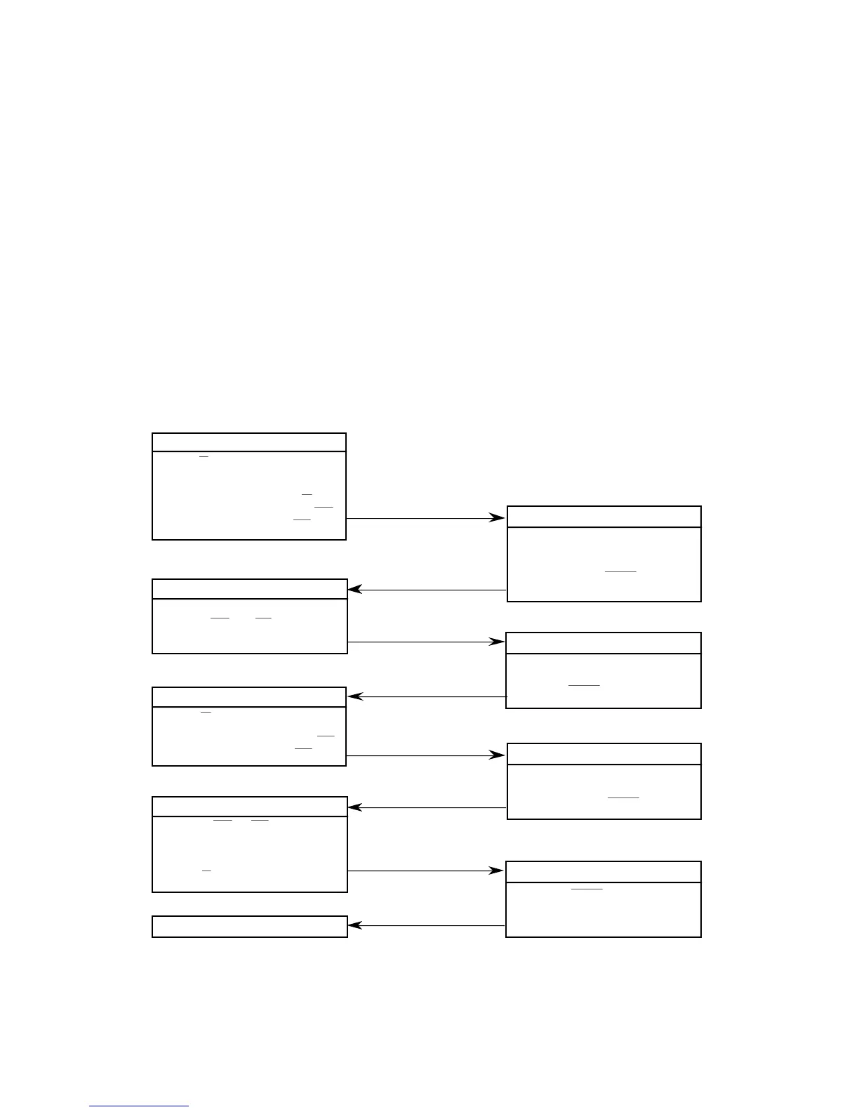
5.1.3 Read-Modify-Write Cycle.
The read-modify-write cycle performs a read operation, modifies the data in the arithmetic
logic unit, and writes the data back to the same address. The address strobe (AS ) remains
asserted throughout the entire cycle, making the cycle indivisible. The test and set (TAS)
instruction uses this cycle to provide a signaling capability without deadlock between
processors in a multiprocessing environment. The TAS instruction (the only instruction
that uses the read-modify-write cycle) only operates on bytes. Thus, all read-modify-write
cycles are byte operations. The read-modify-write flowchart shown in Figure 5-8 and the
timing diagram in Figure 5-9, applies to the MC68000, the MC68HC000, the MC68HC001
(in 16-bit mode), the MC68EC000 (in 16-bit mode), and the MC68010.
) PLACE FUNCTION CODE ON FC2–FC0
) PLACE ADDRESS ON A23–A1
) ASSERT ADDRESS STROBE (AS)
) ASSERT UPPER DATA STROBE (UDS)
OR LOWER DATA STROBE (LDS)
) PLACE DATA ON D7–D0 OR D15–D0
) ASSERT DATA TRANSFER
ACKNOWLEDGE (DTACK)
1) REMOVE DATA FROM D7–D0
OR D15–D8
) NEGATE DTACK
) NEGATE UDS AND LDS
) START DATA MODIFICATION
) PLACE DATA ON D7–D0 OR D15–D8
) ASSERT UPPER DATA STROBE (UDS)
OR LOWER DATA STROBE (LDS)
TERMINATE OUTPUT TRANSFER
) NEGATE AS
) REMOVE DATA FROM D7–D0 OR
D15–D8
) SET R/W TO READ
1) STORE DATA ON D7–D0 OR D15–D8
2
) ASSERT DATA TRANSFER
ACKNOWLEDGE (DTACK)
Figure 5-8. Read-Modify-Write Cycle Flowchart
Frees
cale Semiconductor,
I
Freescale Semiconductor, Inc.
For More Information On This Product,
Go to: www.freescale.com
nc...
 Loading...

