N58 Hardware User Guide
Chapter 5 Application Interfaces
Copyright © Neoway Technology Co., Ltd. All rights reserved.
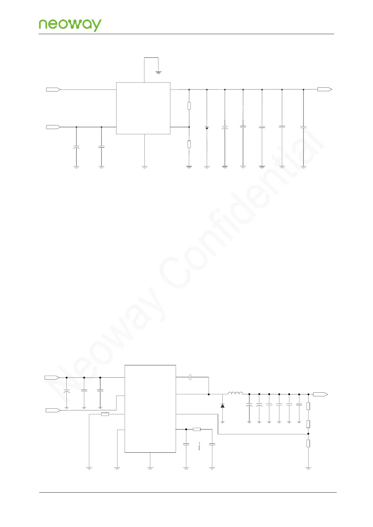
Figure 5-4 Recommended design 3
U1
C1
100 μF
R1
100 kΩ
C2
0.1 μF
R2
47.5 kΩ
C4
470 μF
C5
0.1 μF
TVS
D3
EN
VIN
VOUT
ADJ
C3
10 μF
C6
100 pF
C7
33 pF
GND
GND
PWR_EN
VIN (5V)
VBAT
Design with LDO is simpler and more efficient when the output of the power supply is close to
the VBAT voltage value.
Select an LDO that can output a current that is greater than 2.5 A at U1 to ensure the
performance of the module.
The reverse working voltage VRWM of TVS D3 is 4.5 V, and the peak power Ppp is 2800 W (tp =
8/20 uS). TVS is used for power surge protection. Place TVS close to the input interface of the
power supply so that the power surge voltage is clamped before it enters back-end circuits,
protecting the back-end components and the module.
Place C4 close to the module. A large-capacity aluminum electrolytic capacitor (470 μF or 1000
μF) or tantalum electrolytic capacitor (220 μF or 100 μF) can be selected to improve the
instantaneous large current freewheeling capability of the power supply. Its withstand voltage
must be greater than 2 times the voltage of the power supply.
Place low-ESR bypass capacitors (C3, C5, C6, and C7) close to the module to filter out high-
frequency interference from the power supply.
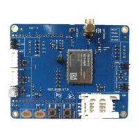
The recommended 5.5 V–24 V input design is as follows.
Figure 5-5 Recommended design 4
VIN
EN
RT/CLK
P-PAD
GND
BOOST
SW
FB
COMP
R1
47.5KΩ
12KΩ
100pF 0.01uF
L1
3.3uH
0.1uF
VBAT
470uF
100uF 22uF
0.1uF 100pF 33pF
1kΩ
47.5kΩ
12kΩ
SS36
VIN
(5.5V-24V)
C1
100uF
C2
22uF
C3
0.1uF
D1
C4 C5
C6
C7
C8
C9 C10 C11
C12
R2
R3
R4
R5
PWR_EN