N58 Hardware User Guide
Chapter 5 Application Interfaces
Copyright © Neoway Technology Co., Ltd. All rights reserved.
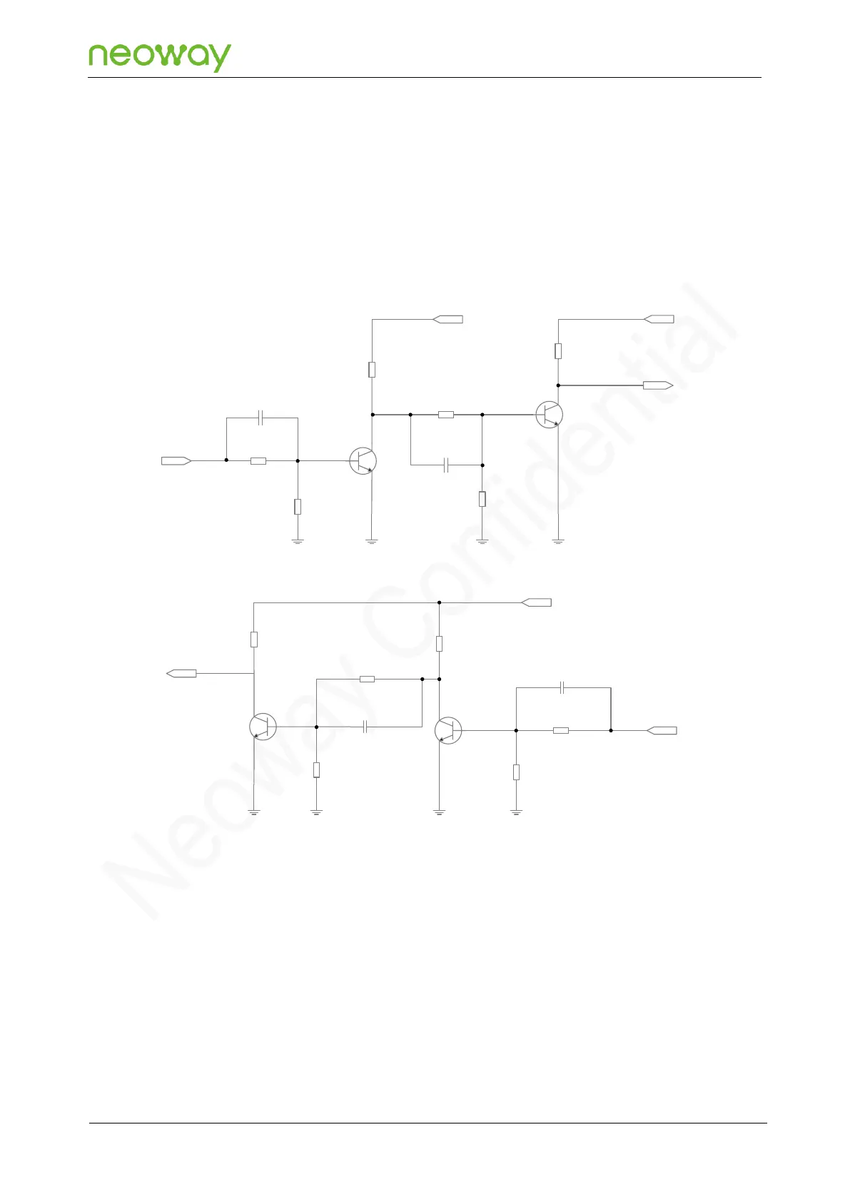
− EN is the enable pin, and is triggered by an input level that is greater than VL-0.2 V. In the
preceding figure, EN is directly connected to VDD_1P8, and the level shifting chip is always
working.
If the UART interface baud rate is lower than or equal to 115200 bps, it is recommended to use
level shifting circuit 2 (see Figure 5-21) for UART interface TXD and RXD and is recommended
to use level shifting circuit 3 (see Figure 5-22) for UART interface CTS and RTS.
Figure 5-21 Recommended level shifting circuit 2
C1
C2
10pF
UART_RXD
10 kΩ
100 kΩ
10 kΩ
VDD_1P8
10kΩ
10pF
100 kΩ
4.7 kΩ
Q1
Q2
MCU_TXD
R4
R1
R6
R5
R2
R3
C1
C2
10pF
UART_TXD
4.7 kΩ
R2
10 kΩ
VDD_1P8
10kΩ
10pF
100kΩ
4.7 kΩ
Q1
Q2
MCU_RXD
VCC_IO
R4
R1
R5
R6
R3
22 kΩ
Related components:
Q1/Q2: MMBT3904 or MMBT2222. High-rate transistors are better.
MCU_TXD and MCU_RXD are the sending and receiving interfaces of the MCU, respectively. TXD
and RXD are the sending and receiving interfaces of the module, respectively. VCC_IO is the IO
voltage of the MCU, and VDD_1P8 is the IO voltage of the module.