N58 Hardware User Guide
Chapter 5 Application Interfaces
Copyright © Neoway Technology Co., Ltd. All rights reserved.
Note the DC resistance of ferrite beads because overlarge DC resistance will consume
excessive audio power, because audio output devices generally have a small impedance. In
principle, the DC resistance of ferrite beads is as small as possible. A ferrite bead with a DC
resistance lower than 0.1 Ω is recommended.
PCB design guidelines:
If the output audio power is large, a large current will occur on the traces, and the PCB needs to
be designed with sufficient width (recommended cable width: 0.5 mm). Isolate the traces from
digital signals and clocks as well as other analog signal cables. Avoid crossing audio cables with
other cables. Reserve enough ground holes and ground protection.
The antenna must be far away from audio traces to reduce radiation interference. Power traces
must not be parallel to audio traces, and should be as far away from audio traces as possible.
Differential audio traces comply with the rules of differential traces.
Reference Design of the External Power Amplifier
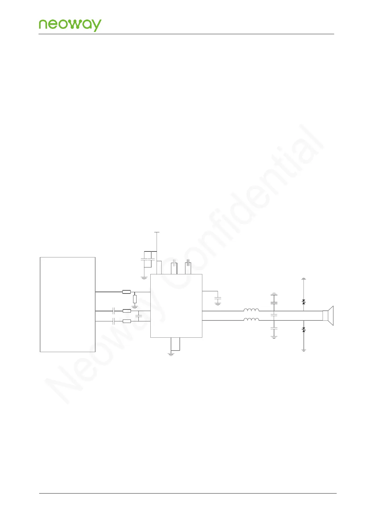
Figure 5-30 Reference design of the external power amplifier
L1
L2
INP
INN
SHDN
VDD
PVDD
VOP
VON
GND
GND
D1
D2
R1
100Ω
C3
C4C5
100nF
VBAT
C6
2.2µF
N58 Module
GPIO
SPK_P
SPK_N
Audio Amplifier
4.7uF
68nF
68nF
C2
C7
2.2µF
VDD
C1P
C1N
C2P
C2N
C8
4.7µF
C9
C10
C11
100pF
100pF
100pF
R2
100kΩ
R3
R4
3kΩ
220pF
3kΩ
C1
Schematic design guidelines:
Connect the SPK output of the N58 module to the power amplifier with differential connections,
and select a power amplifier that can support differential input for the audio power amplifier.
Note that the over-current capability of L1 and L2 must meet the current requirements at the
maximum power. DCR is recommended to be less than 100 mΩ.
PCB design guidelines:
The audio input and output signal cable width must be at least 0.5 mm.