Hardware description
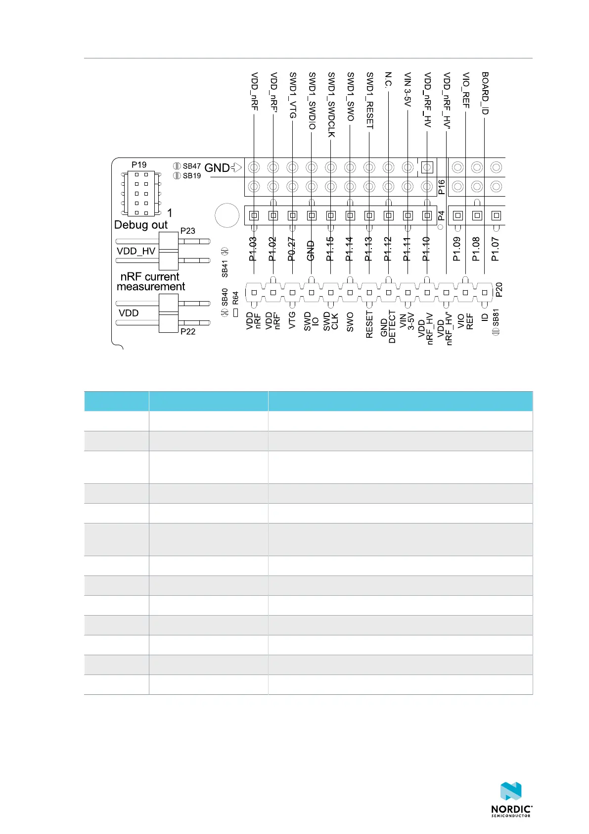
Figure 31: Debug output connector P20
Pin number Signal Description
1 VDD_nRF Application nRF5340 SoC power domain
2 VDD_nRF´ Main nRF5340 DK power domain
3 SWD1_VTG Voltage supply from external target that is used as an enable
signal for activating SWD1
4 SWD1_SWDIO SWD data line
5 SWD1_SWDCLK SWD clock line
6 SWD1_SWO The SWO line is not used for programming and debugging
over SWD
7 SWD1_RESET Reset line
8 N.C. Not used
9 VIN3-5V Voltage supply
10 VDD_nRF_HV nRF5340 DK VBAT power domain for current measurement
11 VDD_nRF_HV´ Main VBAT power domain
12 VIO_REF GPIO voltage reference input
13 BOARD_ID DK ID resistor
Table 9: Pinout of connector P20 for programming external targets
4406_638
31
 Loading...