Display
PRELIMINARY INFORMATION
Jetson Orin NX Series and Jetson Orin Nano Series DG-10931-001_v1.1 | 54
Trace loss characteristic:
dB/in. @ 6GHz
dB/in. @ 3GHz
dB/in. @ 1.5GHz
The max length (delay) is derived based
on this characteristic. The length (delay)
constraint must be re-defined if the loss
characteristic is changed. See Note 1.
Min Trace spacing (Pair-Pair)
Stripline: 2.1
Stripline: 1.4b/2.0
Microstrip: 2.1
Microstrip: 1.4b/2.0
For Stripline, this is 3x of the thinner of
above and below.
Trace spacing (Main link to DDC)
Stripline
Microstrip
For Stripline, this is 3x of the thinner of
above and below.
Max Total Delay (2.1)
Stripline (4x spacing)
Microstrip (7x spacing)
Propagation delay: 6.9ps/mm
assumption for Stripline, 5.9ps/mm for
Microstrip.
Max Total Delay (1.4b/2.0)
Stripline
Microstrip (5x spacing)
Microstrip (7x spacing)
101 (700)
88.5 (525)
101 (600)
Propagation delay: 6.9ps/mm
assumption for Stripline, 5.9ps/mm for
Microstrip.
Max intra-pair (within pair) skew
Max inter-pair (pair to pair) skew
Max GND transition via distance
For signals switching reference layers,
add one or two ground stitching vias. It is
recommended they be symmetrical to
signal vias.
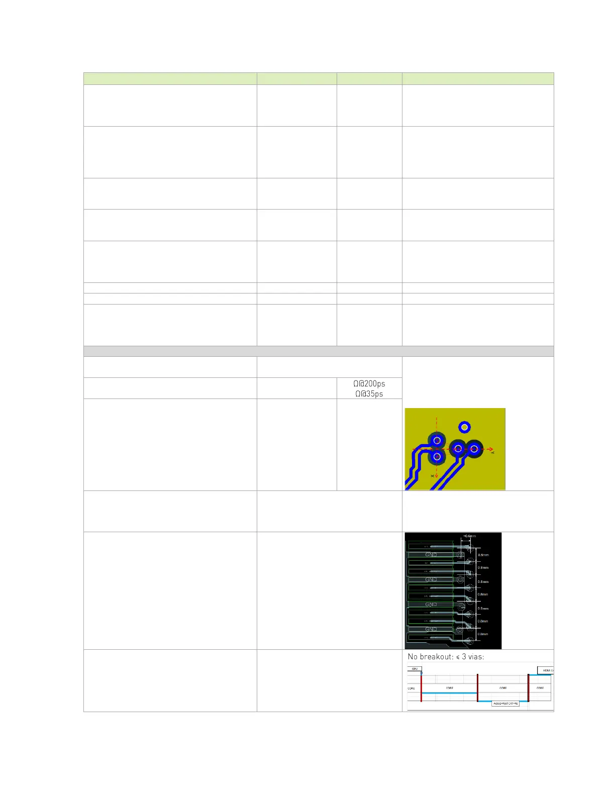
- Y-pattern is recommended
- keep symmetry
Xtalk suppression is the best by Y-
pattern. Also it can reduce the limit of
pair-pair distance. Need review
(NEXT/FEXT check) if via placement is
not Y-pattern.
Recommended via dimension
drill/pad
Antipad
via pitch
Place GND via as symmetrically as
possible to data pair vias. Up to four
signal vias (2 diff pairs) can share a
single GND return via
GND via is used to maintain return path,
while its Xtalk suppression is limited
The break-in trace to the connector pin
via should be routed on the BOTTOM in
order to avoid via stub effect
Equal spacing (0.8mm) between
adjacent signal vias.
The x-axis distance between signal and
GND via should be > 0.6mm
Max # of vias
PTH via
u-via
2 if all vias are PTH via
Not limited if total channel loss
meets IL spec.
 Loading...


