Display
PRELIMINARY INFORMATION
Jetson Orin NX Series and Jetson Orin Nano Series DG-10931-001_v1.1 | 55
Breakout on the same layer as main
long via stub requires review (IL and
resonance dip check)
The main route via dimensions should comply with the via structure rules (See via
section)
See topology in Figure 9-7
For the connector pin vias, follow the rules for the connector pin vias (See via section)
The traces after main route via should be routed as 100 as uncoupled
50ohm SE traces on PCB top or bottom.
Max distance from RPD to main trace (seg B)
Max distance from AC cap to RPD stubbing
point (seg A)
Max distance between ESD and signal via
Example of a case where space is limited for
placing components.
Max via distance from BGA
must be placed before pull-down
resistor
The distance between the AC cap and the
HDMI connector is not restricted.
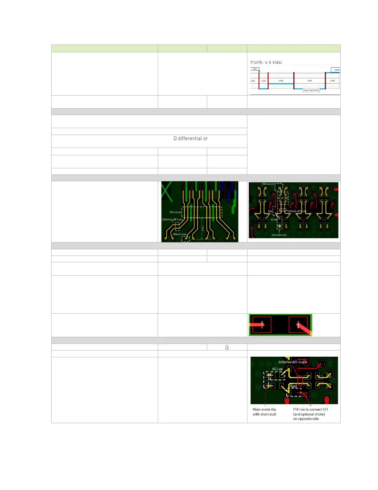
Placement
PTH design
Micro-via design
Place cap on bottom layer if main route
above core
Place cap on top layer if main route
below core
Not Restricted
GND (or PWR) void under/above the
cap is needed. Void size = SMT area +
1x dielectric height keepout distance
Pull-down Resistor (RPD), choke/FET
Must be placed after AC cap
Same layer as AC cap. The FET and
choke can be placed on the opposite
layer thru a PTH via
 Loading...


