Display
PRELIMINARY INFORMATION
Jetson Orin NX Series and Jetson Orin Nano Series DG-10931-001_v1.1 | 56
Choke between RPD and FET choke
Max trace Rdc
Max trace length
Can be choke or Trace. Recommended
option for HDMI2.0 HF1-9 improvement.
GND/PWR void under/above cap is
preferred
Common-mode Choke (Not recommended only used if absolutely required for EMI issues)
See Chapter 17 for details on CMC if implemented.
ESD (On-chip protection diode can withstand 2kV HMM. External ESD is optional. Designs should include ESD footprint as a stuffing
option)
Max junction capacitance
(IO to GND)
e.g. Texas Instruments
TPD4E02B04DQAR
Pad right on the net instead of trace
stub
After pull-down resistor/CMC and
before RS
GND/PWR void under/above the cap is
needed. Void size = 1 mm x 2 mm for
one pair
Series Resistor (RS): Series resistor on P/N path for HDMI 2.0 but not required for HDMI 2.1 (Mandatory to meet HDMI 2.0
Compliance).
± 10%. 0ohm is acceptable if the design
passes the HDMI2.0 HF1-9 test.
Otherwise, adjust the RS value to ensure
the HDMI2.0 tests pass: Eye diagram,
Vlow test and HF1-9 TDR test
After all components and before HDMI
connector
GND/PWR void under/above the RS device is needed. Void size = SMT area + 1x
dielectric height keepout distance.
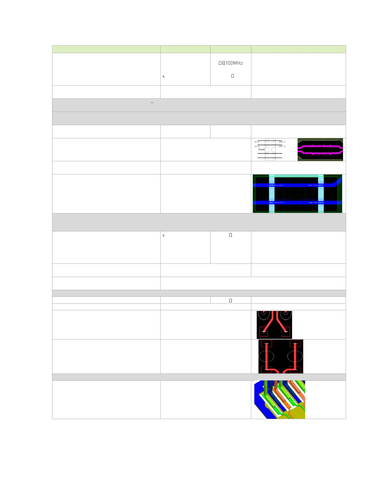
Trace at Component Region
At component region (Microstrip)
Trace entering the SMT pad
Voiding the ground below the signal
lanes 0.1448 (5.7 mil) larger than the
pin itself
 Loading...


