NVIDIA Jetson TX2/TX2i OEM Product Design Guide
JETSON TX2/TX2i OEM PRODUCT | DESIGN GUIDE | 20180618 14
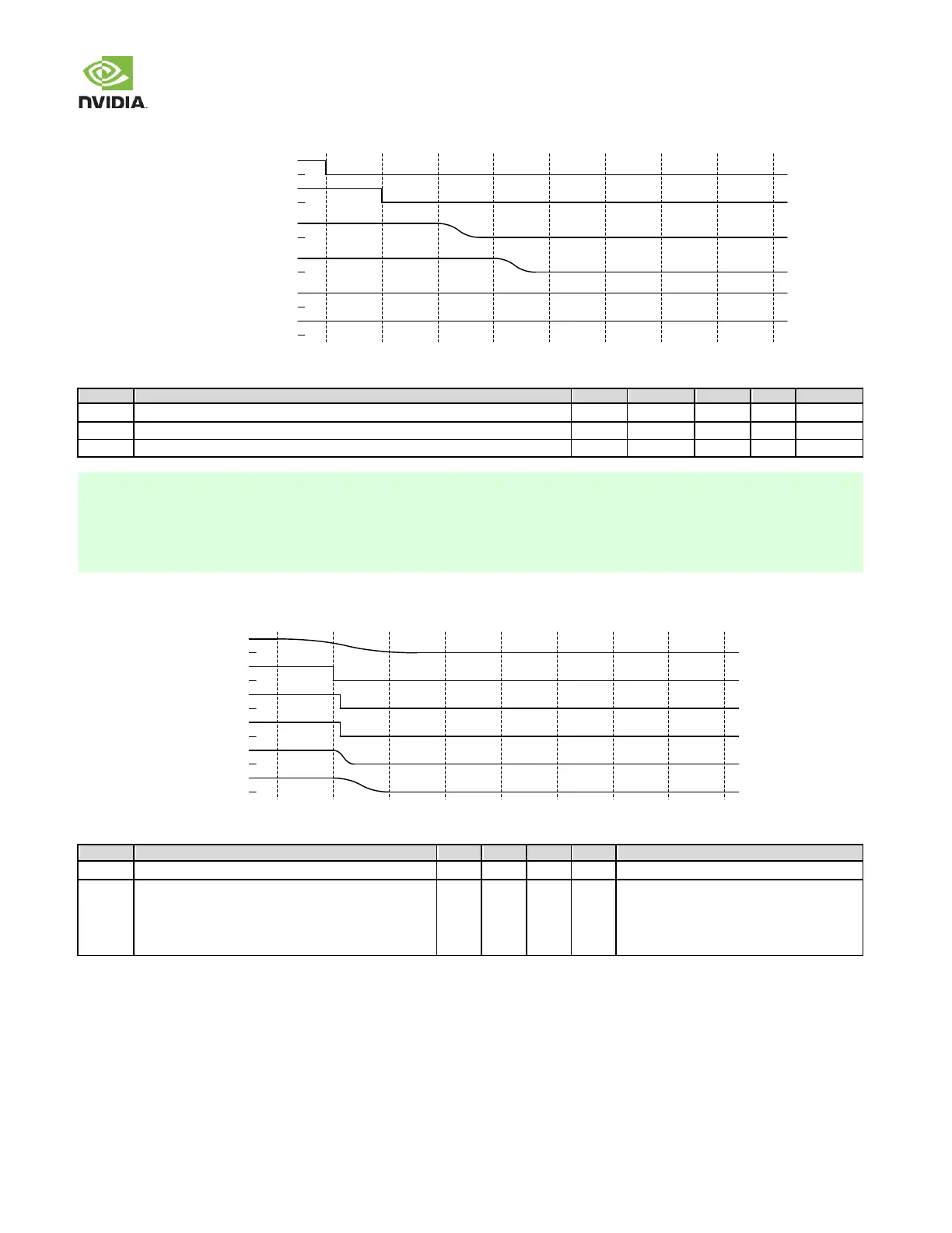
Figure 5. Power Down Sequence (Controlled Case)
CARRIER_PWR_ON
VIN_PWR_BAD#
VDD_IN
Carrier Board System Power (1.8V
used for pins shared w/Jetson module)
Jetson Module System Power (Main 1.8V
rail most IF pins are associated with)
RESET_OUT#
1 2 3 4 5 6 7 8 9
Table 9. Power Down Sequence Timing Relationships (Controlled Case)
RESET_OUT# active to CARRIER_PWR_ON inactive
CARRIER_PWR_ON inactive to carrier board system power off
CARRIER_PWR_ON inactive to the module System Power (main 1.8V rail) Off
1. Measured from RESET_OUT# active to CARRIER_PWR_ON to inactive ramp down start.
2. Typical value measured using NVIDIA P2597. Measured from CARRIER_PWR_ON to carrier board VDD_1V8 ramp down
start. Carrier board dependent.
3. Typical value measured using NVIDIA P2597. Measured from CARRIER_PWR_ON ramp down start to the module main
1.8V ramp down start.
Figure 6. Power Down Sequence (Uncontrolled Power Removal Case)
CARRIER_PWR_ON
VIN_PWR_BAD#
VDD_IN
Carrier Board System Power
Jetson Module System Power
RESET_OUT#
1 2 3 4 5 6 7 8 9
Table 10. Power Down Sequence Timing Relationships (Uncontrolled Power Removal Case)
VDD_IN Removed in uncontrolled manner
asserted to start uncontrolled power-down sequence.
RESET_OUT# & CARRIER_PWR_ON are driven low via
PMIC sequence soon after. Carrier board power & the
module power begin to ramp down.
Carrier board power (mainly 1.8V rail
associated with interface pins connected to
the module) should ramp down faster so it is
off before the module main 1.8V rail is off.
Removal of the VDD_IN/VDD_MUX supply causes VIN_PWR_BAD# to go active w hich causes the module to initiate a
controlled shut dow n. The controlled shut dow n takes ~20ms to complete so the internal PMIC supply needs to stay above
~2.9v for >~20ms. The USB0_OTG_ID pin is a pin w hich can be monitored to see the state of the internal PMIC supply level.