NVIDIA Jetson TX2/TX2i OEM Product Design Guide
JETSON TX2/TX2i OEM PRODUCT | DESIGN GUIDE | 20180618 13
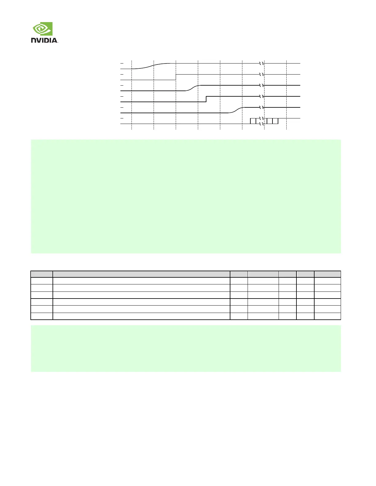
Figure 4. Power Up Sequence – Auto-Power-On Case (Jetson TX2i in P2597_B04)
CARRIER_PWR_ON
VIN_PWR_BAD#
VDD_IN
Carrier Board VDD_1V8 (note 1)
Jetson module System Power (Main 1.8V
rail most IF pins are associated with)
1 2 3 4 5 6 7
RESET_OUT# (note 2)
8
1. The 1.8V supply on the carrier board associated with MPIO pins common to the module must not be enabled unless the
module main 1.8V rail is on. In addition, the carrier board should keep RESET_OUT# low until this 1.8V supply is valid.
On the P2597, this is accomplished by connecting the VDD_1V8 supply PGOOD signal to RESET_OUT#.
2. Inactive when both PMIC Reset is inactive (high) & VDD_1V8 PGOOD is active (high)
3. POWER_BTN# not used for this power-up sequence, but if Jetson TX2i is used in P2597_B04 compatible motherboard,
system will power off if POWER_BTN# is asserted (power-button pressed or equivalent) and power-on sequence will
occur again once POWER_BTN# is de-asserted. This is due to the difference in the PMIC power on signal (edge triggered
on Jetson TX2 PMIC & level sensitive on Jetson TX2i. When Jetson TX2i is used in a P2597_C02 compatible carrier board,
logic on the carrier board simulates edge triggered power-on so the power button will function the same as for Jetson
TX2.
4. During run time if any module I/O rail is switched OFF or ON, the following sequences should be performed. Violating
these sequences will result in extra in-rush current during the rail transition.
- OFF Sequence: The associated NO_IOPOWER bit in the PMC APBDEV_PMC_NO_IOPOWER_0 register must be enabled before the
I/O Rail is powered OFF
- ON Sequence. After an I/O Rail is powered ON, the associated NO_IOPOWER bit in the PMC APBDEV_PMC_NO_IOPOWER_0
1. Typical value using NVIDIA P2597, measured from VDD_IN ramp start to VIN_PWR_BAD# inactive start. Carrier board
dependent.
2. Typical value measured using NVIDIA P2597. Carrier board dependent
3. Typical value using P2597. Carrier board dependent.
4. User Dependent if RESET_IN# connected to button. Otherwise, carrier board dependent. Not shown in P ower up
sequence figure.