NVIDIA Jetson TX2/TX2i OEM Product Design Guide
JETSON TX2/TX2i OEM PRODUCT | DESIGN GUIDE | 20180618 31
To GND Single Ended for P & N
Trace Impedance differential / Single Ended
Trace Spacing (Stripline/Microstrip) Pair Pair
To plane & capacitor pad
To unrelated high-speed signals
Trace loss characteristic @ 2.5GHz
The following max length is derived based on this
characteristic. See note 3
Breakout region (Max Length)
Minimum width and spacing. 4x or wider
dielectric height spacing is preferred
Max PCB via distance from the BGA
Max distance from BGA ball to first PCB via.
PCB within pair (intra-pair) skew
Do trace length matching before hitting
discontinuities
Within pair (intra-pair) matching between
subsequent discontinuities
Differential pair uncoupled length
Place GND vias as symmetrically as possible to data pair vias. GND via distance should be placed
less than 1x the diff pair via pitch
Max # of Vias PTH Vias
Micro-Vias
2 for TX traces & 2 for RX trace
No requirement
Longer via stubs would require review
Routing signals over antipads
Only required for TX pair when routed to connector
Location (max length to adjacent discontinuity)
Discontinuity such as edge finger, component pad
Voiding the plane directly under the pad 3-4
mils larger than the pad size is
recommended.
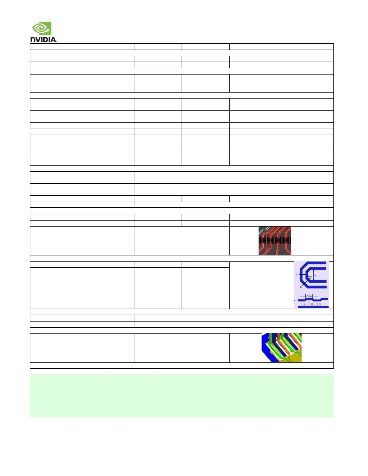
S1 must be taken care in
order to consider Xtalk to
adjacent pair
Dimension Min A Spacing
Min B, C Length
Min Jog Width
Routing signals over antipads
When signal pair approaches Vias, the maximal trace length across the void on the plane is 50mil.
Voiding the plane directly under the pad 5.7
mils larger than the pad size is
recommended.
Keep critical PCIe traces such as PEX_TX/RX, TERMP etc. away from other signal traces or unrelated power traces/areas or powe r supply components
1. The PCIe spec. has 40-60 absolute min/max trace impedance, which can be used instead of the 50 , ± 15%.
2. If routing in the same layer is necessary, route group TX & RX separately without mixing RX/TX routes & keep distance
between nearest TX/RX trace & RX to other signals 3x RX-RX separation.
3. Longer trace lengths may be possible if the total trace loss is equal to or better than the target. If the loss is greater, the
max trace lengths will need to be reduced.
4. Do length matching before Via transitions to different layers or any discontinuity to minimize common mode conversion.