NVIDIA Jetson TX2/TX2i OEM Product Design Guide
JETSON TX2/TX2i OEM PRODUCT | DESIGN GUIDE | 20180618 32
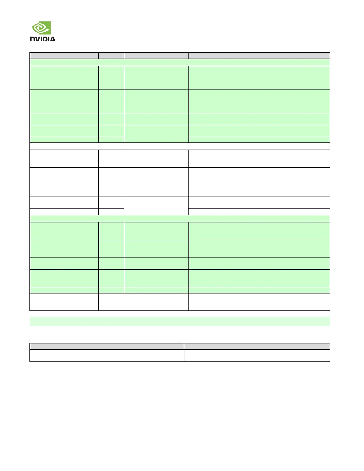
Table 24. PCIE Signal Connections
PCIe Interface #0 (x1 default configuration – x4 optional.
PEX0_TX+/– (Lane 0)
USB_SS1_TX+/– (Lane 1)
PEX2_TX+/– (Lane 2)
PEX_RFU_TX+/– (Lane 3)
Differential Transmit Data Pairs: Connect to TX_P/N pins of PCIe
connector or RX_P/N pin of PCIe device through AC cap according to
supported configuration. Default configuration (x1) uses only Lane 0.
PEX0_RX_+/– (Lane 0)
USB_SS1_RX+/– (Lane 1)
PEX2_RX+/– (Lane 2)
PEX_RFU_RX+/– (Lane 3)
Series 0.1uF capacitors if
device on main PCB.
Differential Receive Data Pairs: Connect to RX_P/N pins of PCIe
connector or TX_P/N pin of PCIe device through AC cap according to
supported configuration. Default configuration (x1) uses only Lane 0.
Differential Reference Clock Output: Connect to REFCLK_P/N pins of
PCIe device/connector
56ullup to
VDD_3V3_SYS on each line
(exists on the module)
PEX Clock Request for PEX0_REFCLK: Connect to CLKREQ pin on
device/connector.
PEX Reset: Connect to PERST pin on device/connector.
PCIe Interface #1 (x1) – (Shared with PCIe Interface #0 lane 2)
Differential Transmit Data Pairs: Connect to TX+/– pins of PCIe
connector or RX_+/– pin of PCIe device through AC cap according to
supported configuration.
Series 0.1uF capacitors if
device on main PCB.
Differential Receive Data Pairs: Connect to RX_+/– pins of PCIe
connector or TX_+/– pin of PCIe device through AC cap according to
supported configuration.
Differential Reference Clock Output: Connect to REFCLK_+/ pins of
PCIe device/connector.
56
VDD_3V3_SYS on each line
(exists on the module)
PEX Clock Request for PEX2_REFCLK: Connect to CLKREQ pin on
device/connector(s)
PEX Reset: Connect to PERST pin on device/connector.
PCIe Interface #2 (x1) – Muxed with USB 3.0 Port #0 on USB_SS0
Differential Transmit Data Pairs: Connect to TX+/– pins of PCIe
connector or RX_+/– pin of PCIe device through AC cap according to
supported configuration.
Series 0.1uF capacitors if
device on main PCB.
Differential Receive Data Pairs: Connect to RX_+/– pins of PCIe
connector or TX_+/– pin of PCIe device through AC cap according to
supported configuration.
Differential Reference Clock Output: Connect to REFCLK_+/ pins of
PCIe device/connector
56
VDD_3V3_SYS on each line
(exists on the module)
PEX Clock Request for PEX1_REFCLK: Connect to CLKREQ pin on
device/connector(s)
PEX Reset: Connect to PERST pin on device/connector(s)
56
VDD_3V3_SYS (exists on the
module)
PEX Wake: Connect to WAKE pins on devices or connectors
CIE IF mapping options.
Table 25. Recommended PCIe observation (test) points for initial boards
One for each of the PCIe TX_+/– output lines used.
Near PCIe device. Connector pins may serve as test points if accessible.
One for each of the PCIe RX_+/– input lines used.
Near the module connector.