NVIDIA Jetson TX2/TX2i OEM Product Design Guide
JETSON TX2/TX2i OEM PRODUCT | DESIGN GUIDE | 20180618 34
Place ground vias as symmetrically as possible to data pair vias
GND via distance should be placed less than 1x the diff pair via pitch
Voiding the plane directly under the pad 3-4 mils larger than the pad size is
recommended
Connector voiding (Required)
The size of voiding can be same as the size of pin pad
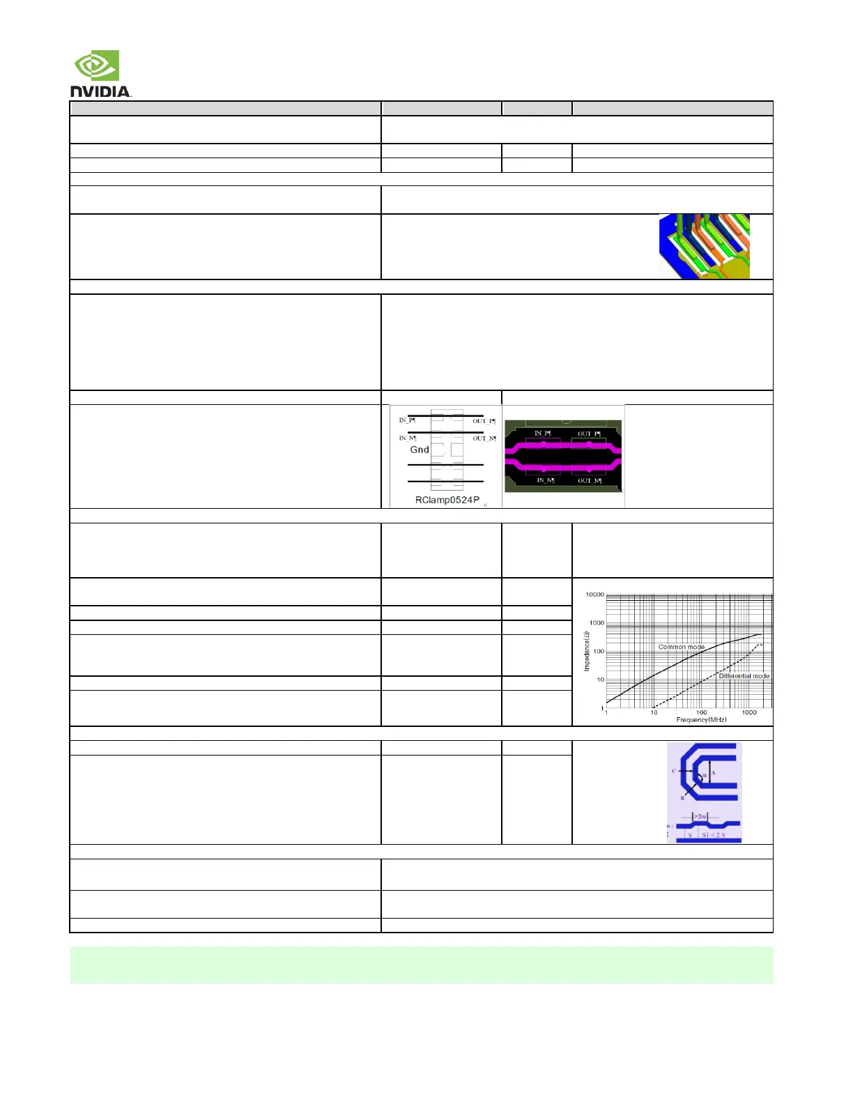
ESD protection device (Optional)
Type: SEMTECH RClamp0524p. Place ESD component near connector.
A design may include the footprints for ESD as a stuffing option. The junction
an ESD component with low capacitance and whose package design is optimized
for high speed links. The SEMTECH ESD Rclamp0524p has been well verified with
its 0.3pF capacitance.
Max distance from ESD Device to Connector
Type: TDK ACM2012D-900-2P. Only if
needed. Place near connector. Refer to
Common Mode Choke Requirement
section.
Location - Max distance from to adjacent discontinuities ex,
connector, AC cap)
Common-mode impedance @ 100MHz Min/Max
Differential TDR impedance
S1 must be
taken care in
order to
consider Xtalk
to adjacent pair
Dimension Min A Spacing
Min B, C Length
Min Jog Width
Where signal pair approaches Vias, maximal trace length across void
on plane is 1.27mm
Keep critical SATA related traces such as SATA_TX/RX, SATA_TERM etc. away from
other signal traces or unrelated power traces/areas or power supply components
If routing to SATA device or SATA connector includes a flex or 2
nd
PCB, the total routing including all PCBs/flexes must be used
for the max trace & skew calculations