NVIDIA Jetson TX2/TX2i OEM Product Design Guide
JETSON TX2/TX2i OEM PRODUCT | DESIGN GUIDE | 20180618 42
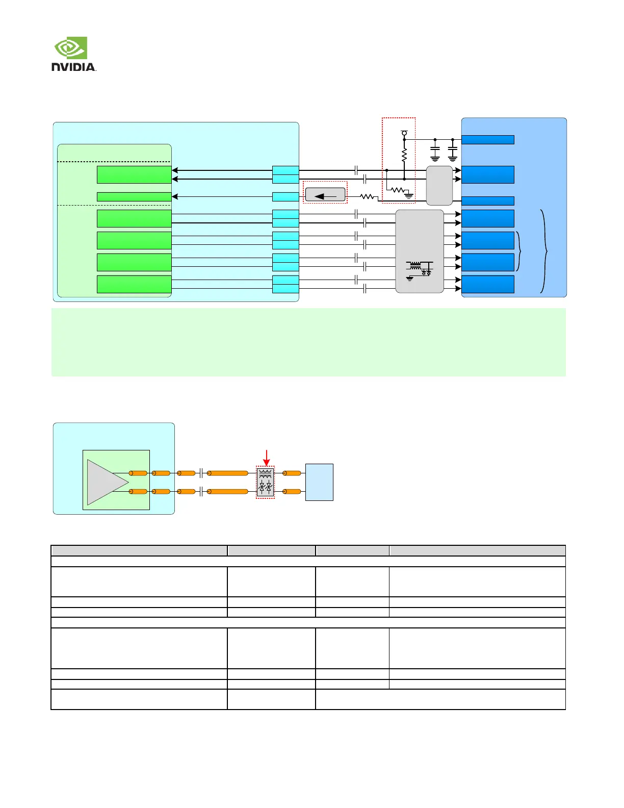
7.2.1 EDP/DP
Figure 24: eDP / DP Connection Example
Jetson TX2/TX2i
Tegra
DPx_AUX_CH+
DPx_AUX_CH
DPx_HPD
DPx_TX2
DPx_TX2
DPx_TX1
DPx_TX1
DPx_TX0
DPx_TX0
DPx_TX3
DPx_TX3
HDMI_DPx_TXDP0
HDMI_DPx_TXDN0
HDMI_DPx_TXDP1
HDMI_DPx_TXDN1
HDMI_DPx_TXDP2
HDMI_DPx_TXDN2
HDMI_DPx_TXDP3
HDMI_DPx_TXDN3
DP_AUX_CHx_P
DP_AUX_CHx_N
EDP
DP[1:0]
DP_AUX_CHx_HPD
eDP / DP Connector
LN2+
LN2
HPD
0.1uF
0.1uF
0.1uF
0.1uF
0.1uF
LN1+
LN1
LN0+
LN0
LN3+
LN3
AUX+
AUX
2-lane 4-lane
Level Shifter
See Note 1
EMI/ESD
1k
EMI/
ESD
100k
100k
3.3V
0.1uF 10uF
See Note 2
+3.3V
0.1uF
0.1uF
0.1uF
0.1uF
0.1uF
B3 6/A33
B3 5/A35
B3 4/A34
G37/D37
G36/D36
F38/C3 8
F37/C3 7
H39/E3 9
H36/E3 6
H35/E35
H38/E3 8
DP0/DP1
1. A Level shifter is required on HPD to avoid the pin from being driven when the module is off. The level shifter must be non-
inverting (preserve the polarity of the HPD signal from the display ).
2. Pull-up/down only required for DP – not for eDP.
3. If EMI devices are necessary, they must be tuned to minimize the impact to signal quality, which must meet the timing &
electrical requirements of the Display Port specification for the modes to be supported. Any ESD solution must also maintain
signal integrity & meet the DisplayPort requirements for the modes to be supported.
eDP Routing Guidelines
Figure 25: eDP / DP (Differential Main Link) Topology
Jetson TX2/TX2i
eDP
Conn
Tegra
Pkg
DP
Driver
P
N
Common Mode
Chokes & ESD
Table 40. eDP / DP Main Link Signal Routing Requirements (Including DP_AUX)
Max Data Rate / Min UI HBR2
HBR
RBR
5.4 / 185
2.7 / 370
1.62 / 617
Number of Loads / Topology
Point-Point, Differential, Unidirectional
Insertion Loss E-HBR @ 0.675GHz
PBR 0.68GHz
HBR 1.35GHz
HBR2 @ 2.7GHz
IL/FEXT plot up to HBR2