NVIDIA Jetson TX2/TX2i OEM Product Design Guide
JETSON TX2/TX2i OEM PRODUCT | DESIGN GUIDE | 20180618 46
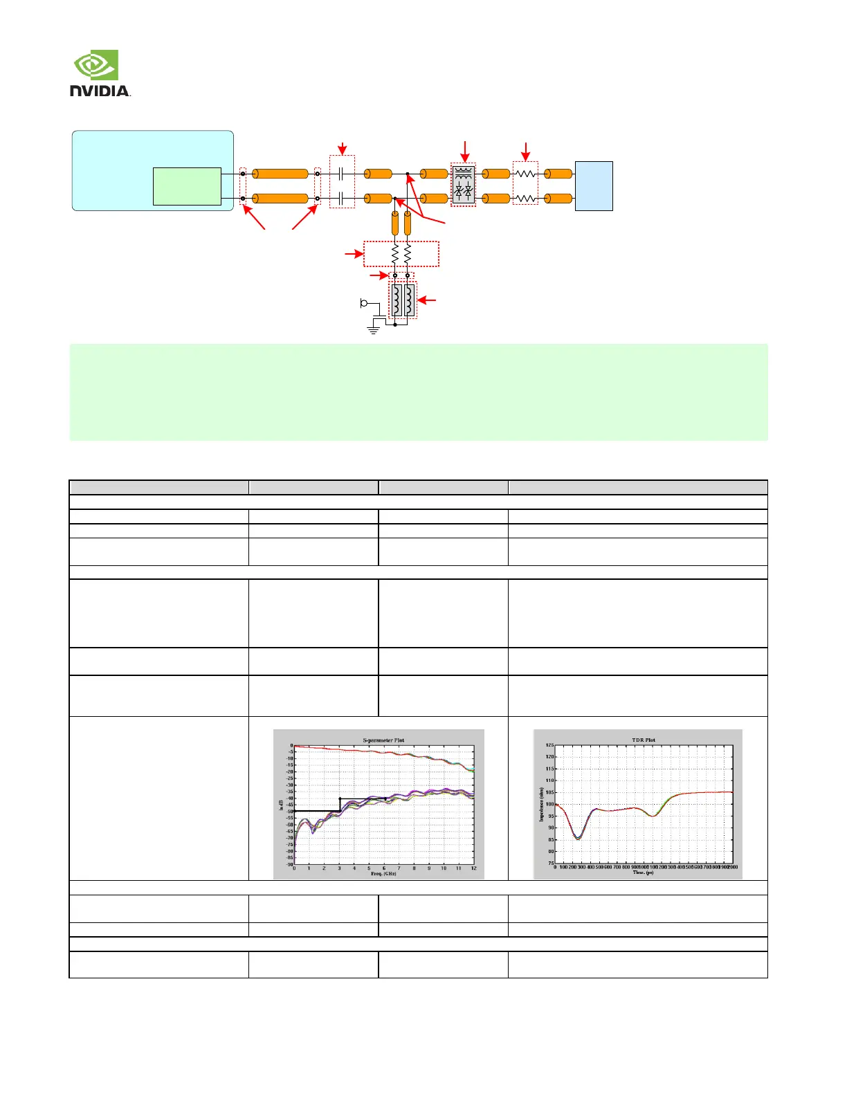
Figure 27: HDMI Clk/Data Topology
Jetson TX2/TX2i
HDMI
Conn
AC
CAP
Seg D Seg F
3.3V
499Ω,
1%
PCB Vias
PCB Vias
0.1uF
0.1uF
R
PD
Common Mode
Chokes & ESD
See Note 1
499Ω,
1%
Seg B Seg E
Seg C
Tegra
-
-
Main Route –
Seg A
* Note 3 * Note 3* Note 3 * Note 3
R
S
(See note 4)
Choke or Trace
See Note 2
1. R
PD
pad must be on the main trace. R
PD
& AC
CAP
must be on same layer.
2. -100MHz) between pull-downs & FET are required for Standard
Technology (through-hole) designs and recommended for HDI designs.
3. The trace after the main-route via should be routed on the Top or Bottom layer of the PCB, and either with 100ohm
differential impedance, or as uncoupled 50ohm Single Ended traces.
4. R
S
series resistor is required. See the R
S
section of the HDMI Interface Signal Routing Requirements table for details.
Table 43. HDMI Interface Signal Routing Requirements
Per lane not total link bandwidth
Unidirectional, Differential
Termination At Receiver
On-board
Differential To 3.3V at receiver
To GND near connector
IL
resonance dip frequency
<= 1.7
<= 2
<= 3
< 6
> 12
dB @ 1GHz
dB @ 1.5GHz
dB @ 3GHz
dB @ 6GHz
GHz
10%-90%. If TDR dip is 75~85ohm that dip width
should < 250ps
dB at DC
dB at 3GHz
dB at 6GHz
PSNEXT is derived from an algebraic summation of the
individual NEXT effects on each pair by the other pairs
Trace Impedance Diff pair
±10for the breakout & main
route is an implementation option.
Trace spacing/Length/Skew
Trace loss characteristic:
dB/in. @ 3GHz
dB/in. @ 1.5GHz
The max length is derived based on this characteristic.
See note 1.