NVIDIA Jetson TX2/TX2i OEM Product Design Guide
JETSON TX2/TX2i OEM PRODUCT | DESIGN GUIDE | 20180618 45
Table 41. eDP Signal Connections
Series 0.1uF capacitors on all lines
eDP/DP Differential CLK/Data Lanes: Connect to matching pins on display
connector. See DP/HDMI Pin Mapping & connection diagram for details.
eDP/DP: Auxiliary Channels: Connect to AUX_CH+/ on display connector.
eDP/DP: Hot Plug Detect: Connect to HPD pin on display connector.
Table 42. Recommended eDP/DP observation (test) points for initial boards
One for each signal line.
Near display connector. Connector pins can be used if accessible.
Test points must be done carefully to minimize signal integrity impact. Avoid stubs & keep pads small & near signal traces
7.2.2 HDMI
A standard DP 1.2a or HDMI V2.0 interface is supported. These share the same set of interface pins, so either Display Port or
HDMI can be supported natively. Dual-Mode DisplayPort(DP++ ) can be supported, in w hich the DisplayPort connector logically
outputs TMDS signaling to a DP-to-HDMI dongle.
7.2.3 HDMI
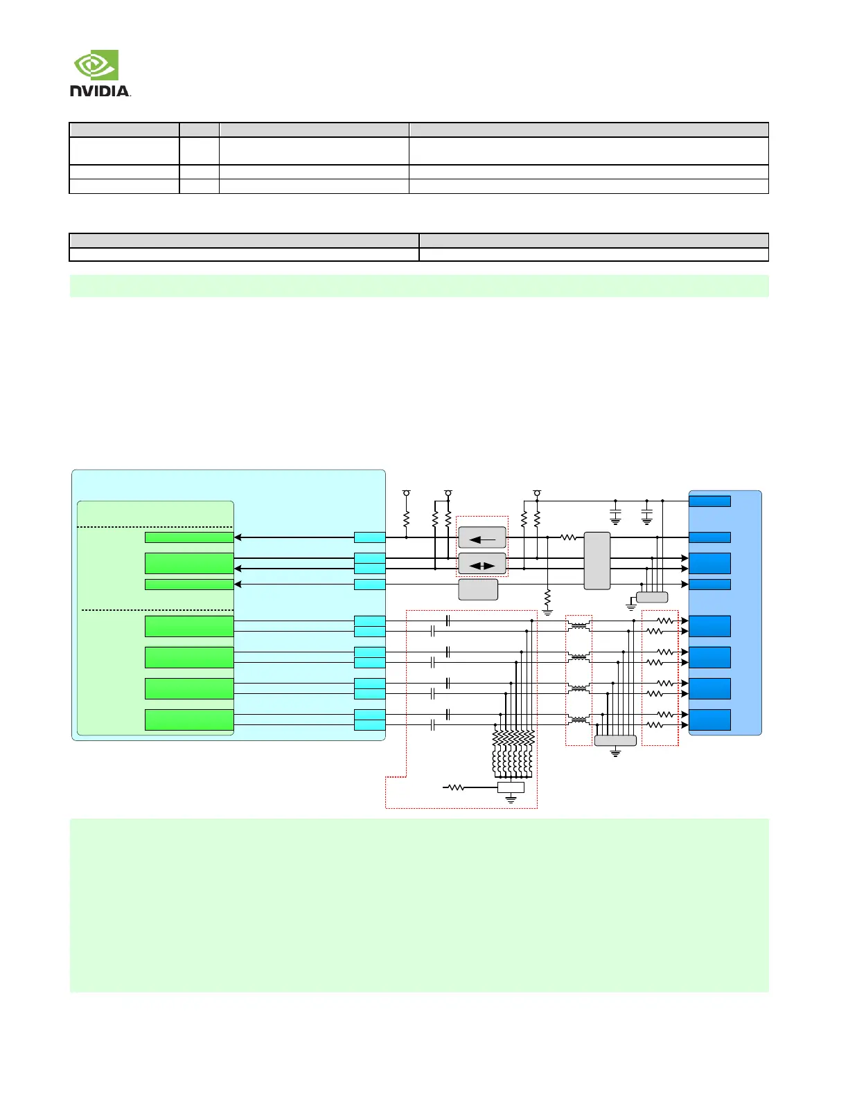
Figure 26: HDMI Connection Example
Jetson TX2/TX2i
CEC Gating
Circuitry
10k
10k
VDD_3V3_SYS
1.8k
1.8k
VDD_5V0_HDMI
Tegra - HDMI
HDMI_DPx_TXDP3
HDMI_DPx_TXDN3
HDMI_DPx_TXDP2
HDMI_DPx_TXDN2
HDMI_DPx_TXDP1
HDMI_DPx_TXDN1
HDMI_DPx_TXDP0
HDMI_DPx_TXDN0
DP_AUX_CH1_P
DP_AUX_CH1_N
DP_AUX_CH1_HPD
eDP
HDMI_DPx
HDMI_CEC
10k
B3 6/A33
B3 5/A35
B3 4/A34
B3 3
G37/D37
G36/D36
F38/C38
F37/C37
H39/E3 9
H36/E3 6
H35/E3 5
H38/E3 8
DPx_HPD
DPx_AUX_CH+
DPx_AUX_CH
HDMI_CEC
DPx_TX2
DPx_TX2
DPx_TX1
DPx_TX1
DPx_TX0
DPx_TX
DPx_TX3
DPx_TX3
FET
Enable
5V0_HDMI_EN
0.1uF
0.1uF
0.1uF
0.1uF
0.1uF
0.1uF
0.1uF
0.1uF
1%
@100MHz
See Note 1
Level Shifter
Level Shifter
VDD_1V8
DP0/DP1
TXD0_P
TXD0_N
TXD1_P
TXD1_N
TXD2_P
TXD2_N
TXC_P
TXC_N
SCL
SDA
HPD
CK+
CK-
D0+
D0-
D1+
D1-
D2+
D2-
CEC
+5V
ESD
100k
0.1uF
HDMI Connector
100k
10uF
EMI
See Note 2
See
Note 2
See Note 3
ESD
R
S
R
S
R
S
R
S
R
S
R
S
R
S
R
S
See
Note 4
CMC
1. Level shifters required on DDC/HPD. Jetson TX2/TX2i pads are not 5V tolerant & cannot directly meet HDMI V
IL
/V
IH
requirements. HPD level shifter can be non-inverting or inverting.
2. If EMI/ESD devices are necessary, they must be tuned to minimize the impact to signal quality, which must meet the
timing & electrical requirements of the HDMI specification for the modes to be supported. See requirements &
recommendations in the related sections of the HDMI Interface Signal Routing Requirements table.
3. The HDMI_DP_TXx pads are native DP pads & require series AC capacitors (AC
CAP
) & pull-downs (R
PD
) to be HDMI
compliant. The 499 pull-downs must be disabled when Tegra is off to meet the HDMI V
OFF
requirement. The
enable to the FET, enables the pull-downs when the HDMI interface is to be used. Chokes between pull-downs & FET are
required for Standard Technology designs and recommended for HDI designs.
4. Series resistors R
S
are required. See the R
S
section of the HDMI Interface Signal Routing Requirements table for details.
5. Tegra supports a single CEC controller that can be associated with one of the display output heads.