NVIDIA Jetson TX2/TX2i OEM Product Design Guide
JETSON TX2/TX2i OEM PRODUCT | DESIGN GUIDE | 20180618 44
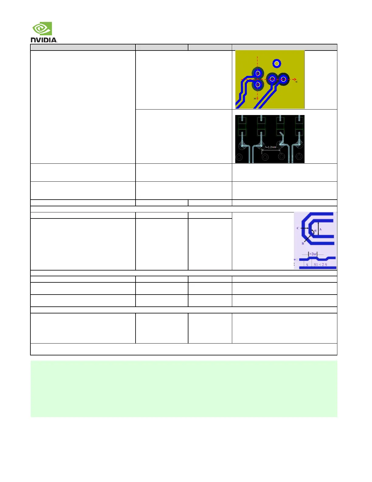
- Y-pattern is recommended
- keep sy mmetry
Xtalk suppression is best using the Y-pattern.
It can also reduce the limit of pair-pair
distance.
For in-line via, the distance from a via of one
lane to the adjacent via from other lane >=
1.2mm center-center.
Place GND via as symmetrically as possible to
data pair vias. Up to 4 signal vias (2 diff
pairs) can share a single GND return via
GND via is used to maintain return path, while its
Xtalk suppression is limited
Max # of Vias PTH vias
Micro Vias
4 if all vias are PTH via
Not limited as long as total channel loss
meets IL spec
S1 must be taken care in
order to consider Xtalk to
adjacent pair
Dimension Min A Spacing
Min B, C Length
Min Jog Width
Max Dist. from A C cap RBR/HBR
to connector HBR2
No requirement
Voiding required
HBR2: Voiding the plane directly under the pad 3-
4 mils larger than the pad size is recommended.
No requirement
Voiding required
HBR2: Standard DP Connector: Voiding
requirement is stack-up dependent. For typical
stack-ups, voiding on the layer under the
connector pad is required to be 5.7mil larger than
the connector pad.
Keep critical eDP related traces including differential clock/data traces & RSET trace away from other signal traces or unrelated power traces/areas or
power supply components
1. For eDP/DP, the spec puts a higher priority on the trace loss characteristic than on the impedance. However, before
selecting for impedance, it is important to make sure the selected stack-up, material & trace dimension can achieve
the needed low loss characteristic.
2. Longer trace lengths may be possible if the total trace loss is equal to or better than the target. If the loss is greater, the
max trace lengths will need to be reduced.
3. The average of the differential signals is used for length matching.
4. Do not perform length matching within breakout region. Recommend doing trace length matching to <1ps before Vias
or any discontinuity to minimize common mode conversion