NVIDIA Jetson TX2/TX2i OEM Product Design Guide
JETSON TX2/TX2i OEM PRODUCT | DESIGN GUIDE | 20180618 48
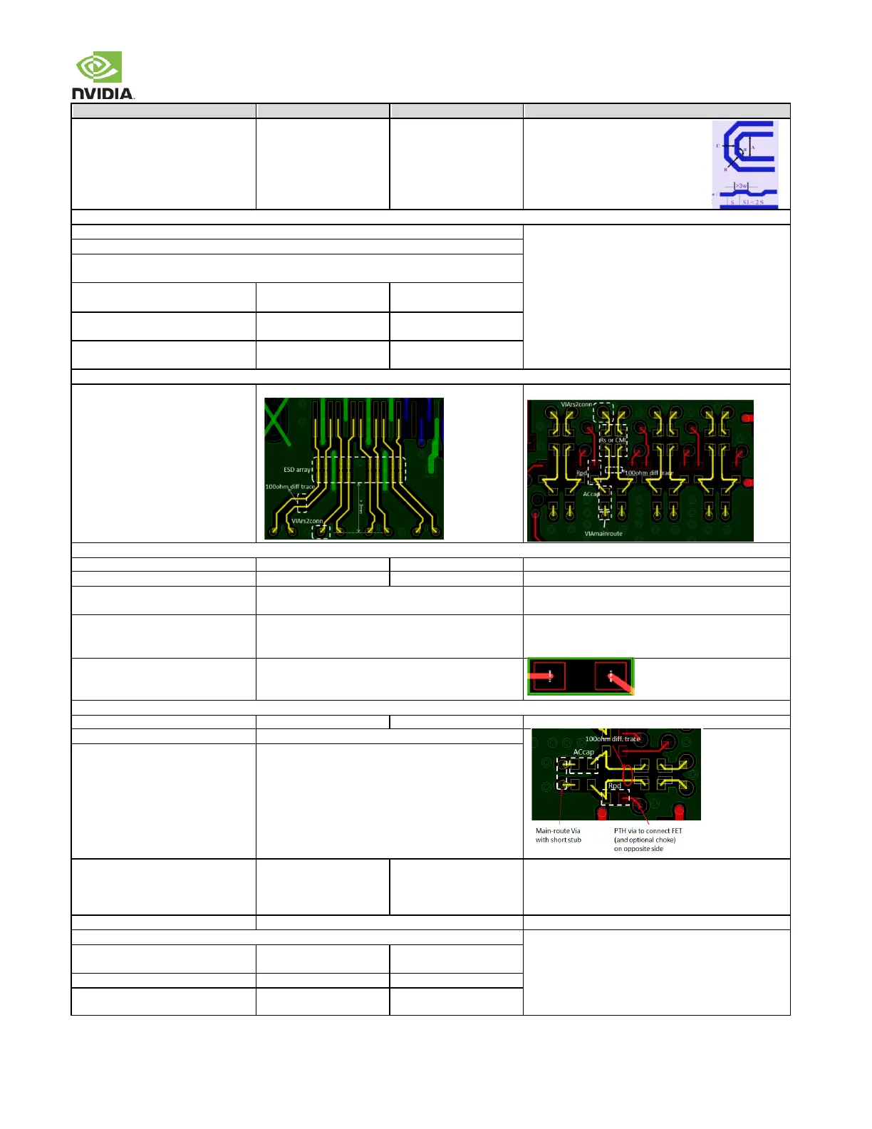
Dimension Min A Spacing
Min B, C Length
Min Jog Width
S1 must be taken care in order to
consider Xtalk to adjacent pair
The main-route via dimensions should comply with the via structure rules (See Via section)
See topology figure above table
For the connector pin vias, follow the rules for the connector pin vias (See Via section)
The traces after main-route via should be routed as 100 as uncoupled 50ohm
Single-ended traces on PCB Top or Bottom.
Max distance from R
PD
to main
trace (seg B)
Max distance from AC cap to RPD
stubbing point (seg A)
Max distance between ESD and
signal via
Example of a case where space is
limited for placing components.
Max via distance from BGA
must be placed before pull-down resistor
The distance between the AC cap and the HDMI
connector is not restricted.
Placement PTH design
Micro-Via design
Place cap on bottom layer if main-route above core
Place cap on top layer if main-route below core
Not Restricted
GND (or PWR) void under/above the cap is needed.
Void size = SMT area + 1x dielectric height keepout
distance
Pull-down Resistor (R
PD
), choke/FET
Must be placed after AC cap
Same layer as AC cap. The FET & choke can be placed
on the opposite layer thru a PTH via
Choke between R
PD
& FET Choke
Max Trace Rdc
Max Trace length
@100MHz
uH@DC-100MHz
m
mm
Can be choke or Trace. Recommended option for
HDMI2.0 HF1-9 improvement.
GND/PWR void under/above cap is preferred
Common-Mode Choke (Stuffing option – not added unless EMI issue is seen)
Common-mode Min
impedance @ 100MHz Max
Differential TDR impedance
90ohm +/-15% @
Tr=200ps (10%-90%)