NVIDIA Jetson TX2/TX2i OEM Product Design Guide
JETSON TX2/TX2i OEM PRODUCT | DESIGN GUIDE | 20180618 49
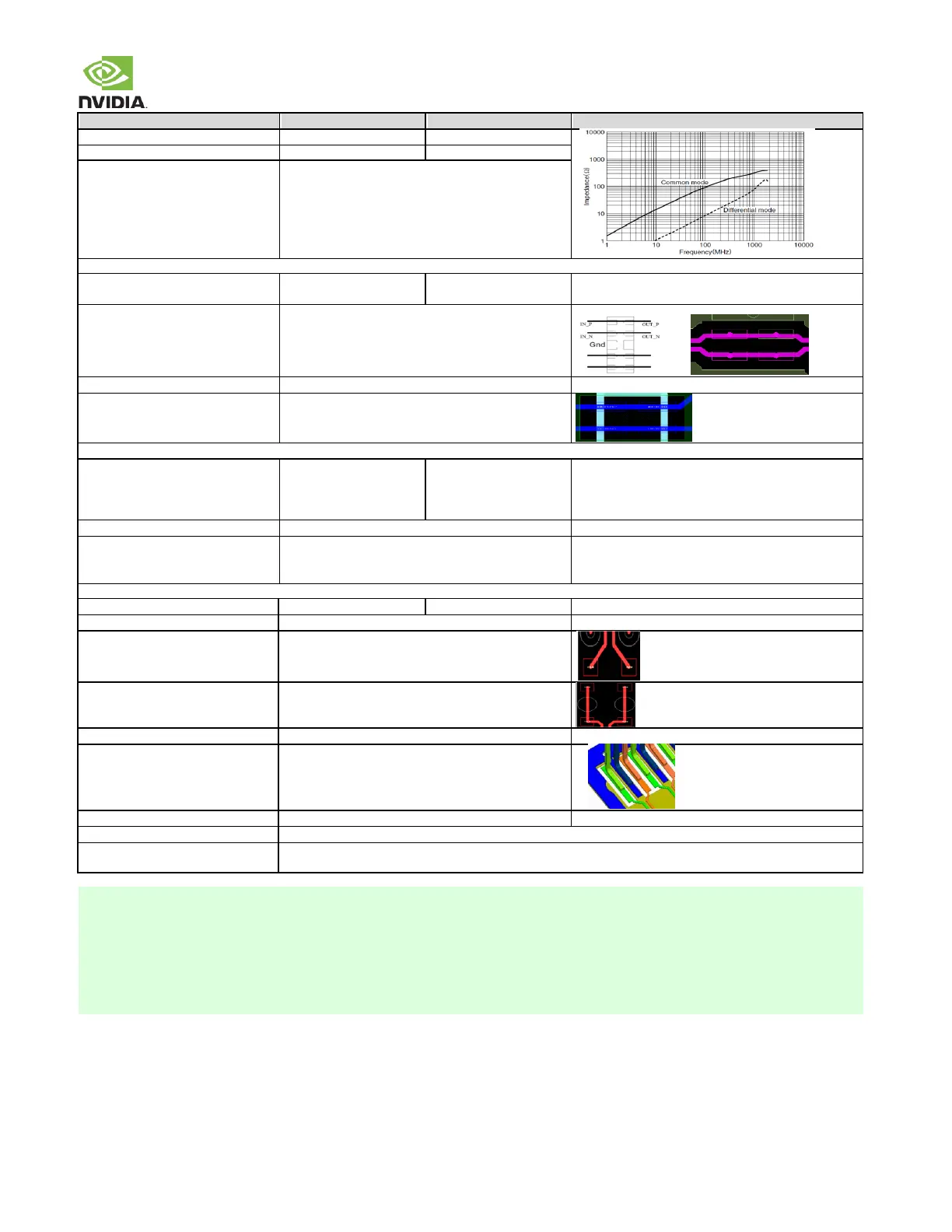
Close to any adjacent discontinuity (< 8mm) such as
connector, via, etc.
ESD (On-chip protection diode is able to withstand 2kV HMM. External ESD is optional. Designs should include ESD footprint as a stuffing option)
Max junction capacitance
(IO to GND)
e.g. ON-semiconductor ESD8040
Pad right on the net instead of trace stub
After pull-down resistor/CMC and before R
S
GND/PWR void under/above the cap is needed. Void
size = 1mm x 2mm for 1 pair
Series Resistor (R
S
) Series resistor on P/N path for HDMI 2.0 (Mandatory)
± 10%. 0ohm is acceptable if the design passes the
HDMI2.0 HF1-9 test. Otherwise, adjust the R
S
value to
ensure the HDMI2.0 tests pass: Eye diagram, Vlow test
and HF1-9 TDR test
After all components and before HDMI connector
GND/PWR void under/above the R
S
device is needed.
Void size = SMT area + 1x dielectric height keepout
distance.
Trace at Component Region
At component region (Microstrip)
Trace entering the SMT pad
Voiding the ground below the signal lanes
0.1448(5.7mil) larger than the pin itself
Routing over voids not allowed except void around device ball/pin the signal is routed to.
Keep critical HDMI related traces including differential clock/data traces & RSET trace away from other signal
traces or unrelated power traces/areas or power supply components
1. Longer trace lengths may be possible if the total trace loss is equal to or better than the target. If the loss is greater, the
max trace lengths will need to be reduced.
2. The average of the differential signals is used for length matching.
3. Do not perform length matching within breakout region. Recommend doing trace length matching to <1ps before vias or
any discontinuity to minimize common mode conversion
4. If routing includes a flex or 2
nd
PCB, the max trace delay & skew calculations must include all the PCBs/flex routing.
Solutions with flex/2
nd
PCB may not achieve maximum frequency operation.