NVIDIA Jetson TX2/TX2i OEM Product Design Guide
JETSON TX2/TX2i OEM PRODUCT | DESIGN GUIDE | 20180618 50
Table 44. HDMI Signal Connections
Termination (see note on ESD)
0.1uF series AC
CAP
PD
(controlled by FET)
EMI/ESD (if required),.
S
(series resistor)
HDMI Differential Clock: Connect to C–/C+ & pins on
HDMI Connector
HDMI Differential Data: Connect to D[2:0]+/– pins. See
DP/HDMI Pin Mapping table and connection diagram.
Module level shifter
100GND on connector
side.
HDMI Hot Plug Detect: Connect to HPD pin on HDMI
Connector
Gating circuitry, See connection figure or reference
schematics for details.
HDMI Consumer Electronics Control: Connect to CEC
on HDMI Connector through circuitry. Tegra supports a
single CEC controller that can be associated with one of
the display output heads.
From the module
level shifter connector pin
HDMI: DDC Interface – Clock and Data: Connect
DP1_AUX_CH+ to SCL & DP1_AUX_CH– to SDA on
HDMI Connector
Adequate decoupling (0.1uF & 10uF recommended) on
supply near connector.
HDMI 5V supply to connector: Connect to +5V on
HDMI Connector.
Any ESD and/or EMI solutions must support targeted modes (frequencies).
Table 45. Recommended HDMI / DP observation (test) points for initial boards
One for each signal line.
Near display connector. Connector pins can be used if accessible.
Test points must be done carefully to minimize signal integrity impact. Avoid stubs & keep pads small & near signal traces
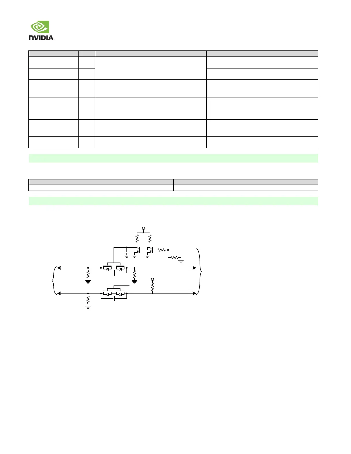
Figure 28: Optional Dual-Mode (DP/HDMI) Connections
100kΩ
100kΩ
100kΩ
100kΩ
Gated
3.3V
0.1uF
0.1uF
DP_MODE*
DP_MODE*
5.0V
10kΩ10kΩ
10kΩ
10kΩ
10nF
CONFIG1
To DP Connector
DP_AUX
DP_AUX*
DP_AUX_CHx_P
DP_AUX_CHx_N
To Jetson
TX2/TX2i
DP Interface Signal Routing Requirements
See eDP/DP Signal Routing Requirements.