NVIDIA Jetson TX2/TX2i OEM Product Design Guide
JETSON TX2/TX2i OEM PRODUCT | DESIGN GUIDE | 20180618 52
Table 48. CSI Configurations
1. Each 2-lane options shown above can also be used for one single lane camera as well
2. Combinations of 1, 2 & 4-lane cameras are supported, as long as any 4-lane cameras match one of the three configurations
above
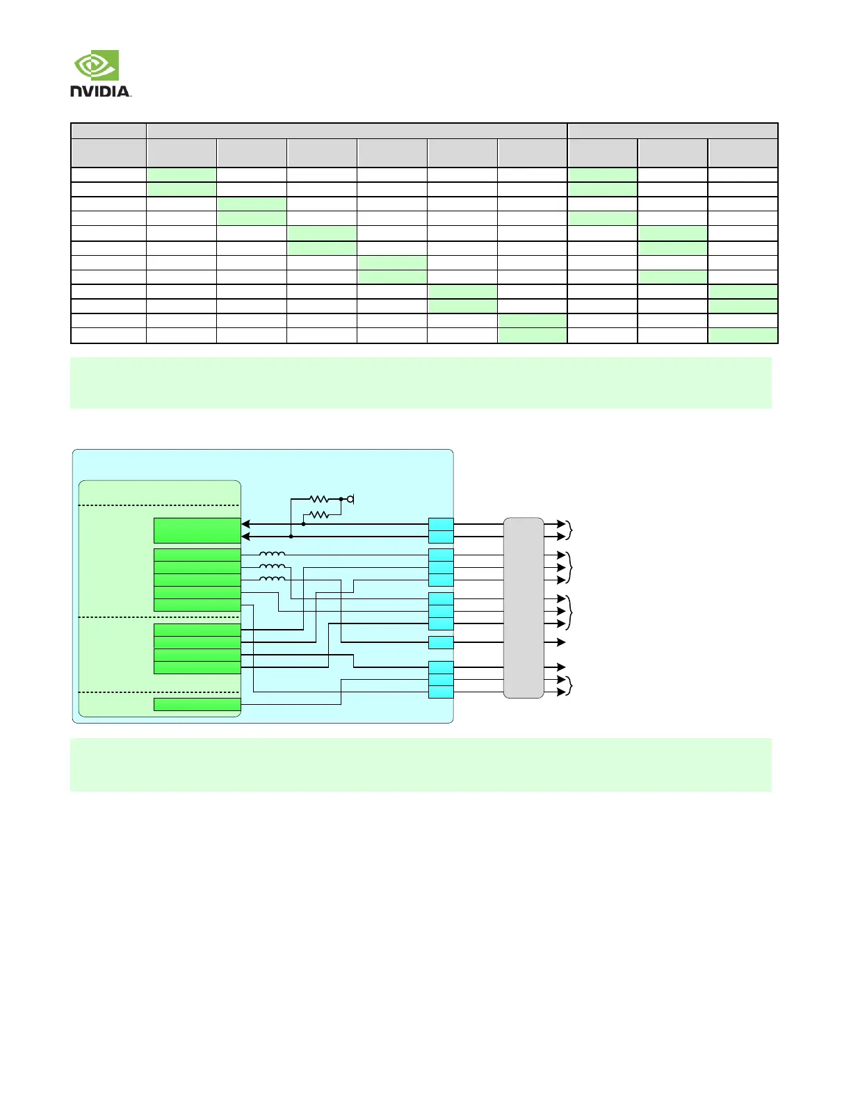
Figure 29: Camera Control Connections
EMI
&
ESD
Jetson TX2/TX2i
1k
1k
VDD_1V8
Camera
I2C
Camera 0
Clock/Control
Camera 1
Clock/Control
Camera
Strobe/Flash
CAM_AF_EN
I2C_CAM_CLK
I2C_CAM_DAT
CAM0_MCLK
GPIO0_CAM0_PWR#
GPIO2_CAM0_RST#
CAM1_MCLK
GPIO1_CAM1_PWR#
GPIO3_CAM1_RST#
CAM2_MCLK
CAM_VSYNC
GPIO4_CAM_STROBE
GPIO5_CAM_FLASH_EN
D6
F9
G8
G7
D7
C6
F7
F8
H7
H8
Tegra
UART/CAM
CAM_I2C_SCL
CAM_I2C_SDA
EXTPERIPH1_CLK
UART5_RTS
GPIO_CAM3
QSPI_SCK
EXTPERIPH2_CLK
SPI
QSPI_CS
QSPI_IO0
QSPI_IO1
E8
GPIO_CAM2
E7
Camera 2 Clock
Misc.
GPIO_SEN5
AO
1. If the module is providing flash control (as shown), GPIO5_CAM_FLASH_EN & GPIO4_CAM_STROBE must be used.
2. Any EMI/ESD devices must be tuned to minimize impact to signal quality and meet the timing & Vil/Vih requirements at
the receiver & maintain signal quality and meet requirements for the frequencies supported by the design .