NVIDIA Jetson TX2/TX2i OEM Product Design Guide
JETSON TX2/TX2i OEM PRODUCT | DESIGN GUIDE | 20180618 54
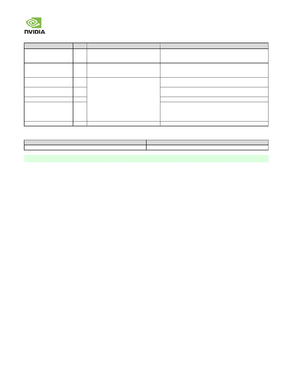
Table 50. Miscellaneous Camera Connections
1k Pull-ups VDD_1V8 (on the module).
See note related to EMI/ESD under MIPI
CSI Signal Connections tables.
Camera I2C Interface: Connect to I2C SCL & SDA pins of imager
120the module) See
note related to EMI/ESD under MIPI CSI
Signal Connections tables.
Camera Master Clocks: Connect to Camera reference clock
inputs.
GPIO1_CAM1_PWR#
GPIO0_CAM0_PWR#
See note related to ESD under MIPI CSI
Signal Connections tables.
Camera Power Control signals (or GPIOs [1:0]): Connect to
powerdown pins on camera(s).
Camera Strobe Enable (or GPIO 4): Connect to camera strobe
circuit unless strobe control comes from camera module.
Camera Flash Enable: Connect to enable of flash circuit
GPIO3_CAM1_RST#
GPIO2_CAM0_RST#
Camera Resets (or GPIO [3:2]): Connect to reset pin on any
cameras with this function. If AutoFocus Enable is required,
connect GPIO3_CAM1_RST# to AF_EN pin on camera module &
use GPIO2_CAM0_RST# as common reset line.
Table 51. Recommended CSI observation (test) points for initial boards
Test points must be done carefully to minimize signal integrity impact. Avoid stubs & keep pads small & near signal traces