Board Interface Connector
MPC5777C EVB User Guide, Rev. 1
16 NXP Semiconductors
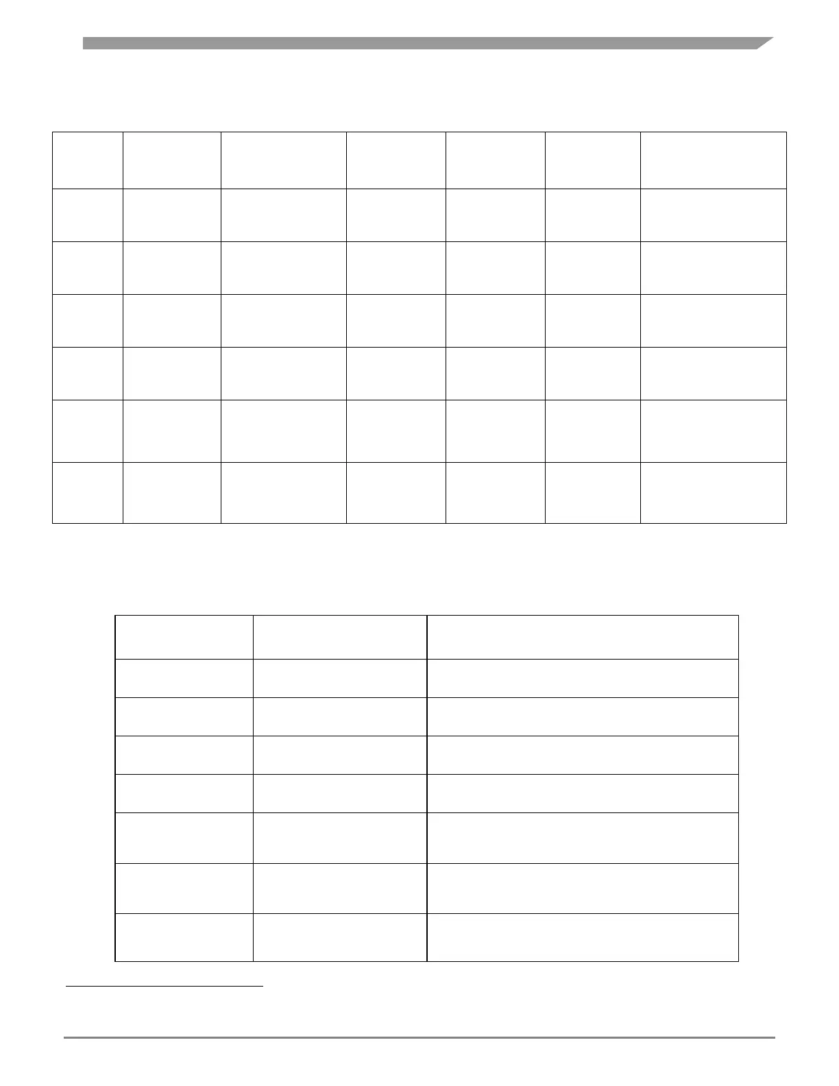
Jumper options to achieve the above power supply modes are shown in Table 8:
Table 8: Jumper options for various power modes
J21
(1V25_SR_MB_SEL)
and J12 (SBC_1V25)
1
2&3 for LV
Linear
Regulator
J21 - 3&4 for
1.25V_SR_OB1 (LR)
J12 - Open
J21 - 5&6 for
1.25V_SR_OB2(SR)
J12 - Open
2&3 for LV
Linear
Regulator
J21 - 3&4 for
1.25V_SR_OB1 (LR)
J12 - Open
J21 - 5&6 for
1.25V_SR_OB2(SR)
J12 – Open
J21 - 1&2 for
1.25V_SR_MB
-OR-
J12-1&2 for SBC_1V25
J21 - 1&2 for
1.25V_SR_MB
-OR-
J12-1&2 for SBC_1V25
The connection of any power domain to a regulator has to be enabled by a dedicated jumper as
described in Table 9.
Table 9:
MCU power selection jumpers (416DC)
Jumper Setting (* - Default)
1-2: 3.3V from onboard Power SBC
2-3: 3.3V from Mother Board*
1-2: 5V from onboard Power SBC
2-3: 5V from Mother Board*
IO Levels in the Mother
Board - VDD_HV_IO_MAIN
1-2: Select 3.3V
2-3: Select 5V*
ADC Analog Supply
Selection
1-2: Select 5V from Linear Regulator*
2-3: Select 5V from Switching Regulator
Connect TRNG, Internal RC
oscillator Supply -
VDDA_MISC
1-2: Connect VDDA_MISC to 5V_SR*
Connect SD ADC supply &
Reference –VDDA_SD,
VRH_SD
J7, 1-2: Connect VDDA_SD*
J8, 1-2: Connect VRH_SD*
Connect eQADC supply &
Reference – VDDA_EQ,
VRH_EQ
J9, 1-2: Connect VDDA_EQ*
J10, 1-2: Connect VRH_EQ*
CAUTION: For 1.25 V source selection, a single jumper must be installed on either J21 or J12, but not on both at a time.

 Loading...


