Address decoding coverage
Safety Manual for MPC5777M, Rev. 1.1
NXP Semiconductors 79
5.4 Test result
Let’s recap the needed steps to perform the test and to analyze the result:
1. A single bit error correction is triggered at the address Ah.
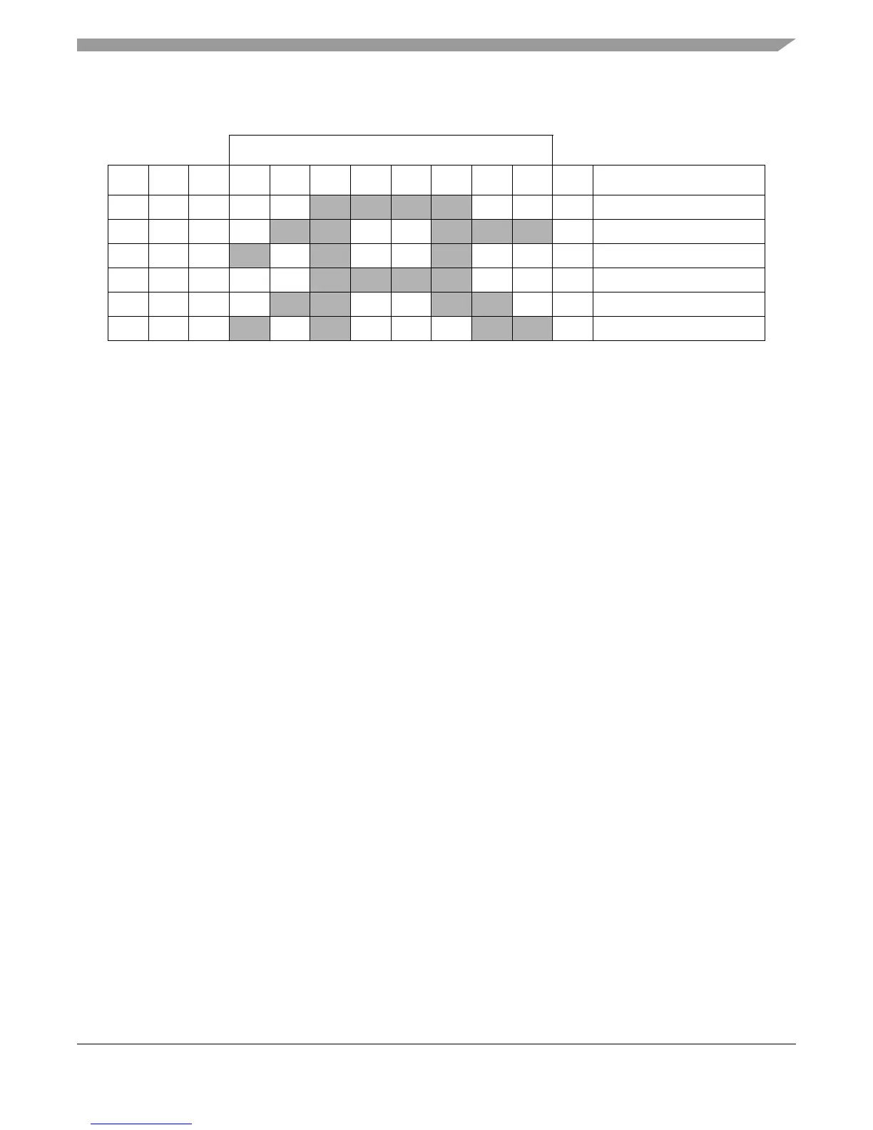
2. Starting from this address and from the RAM architecture, the user shall gather a list of memory
locations which shall be read (for example, greyed cells in Table 12 or Table 16).
3. These locations shall be read to verify if any additional single/double bit error is triggered.
This self-test detects a potential permanent RAM addressing failure if one of the following conditions
appears while reading selected RAM locations:
• a not correctable error bit is detected, or
• multiple single bit errors are detected by the ECC logic and the number of these errors is bigger
than the buffer depth of the MEMU, or
• more than a single bit error are detected on different words of the same word-line (more details on
such a case on section 5.4.1).
As described above additional SBE can be detected by the ECC while the software test runs. In this case
additional iteration of the software test shall be executed considering this new SBE as new hitting address.
5.4.1 Multiple single bit error in the same word-line
A Single Event Effect (SEE) in RAM can cause single bit upset on multiple adjacent words (for example,
Multiple Cell Upset (MCU)).
MCU causes SBEs on different words of the same word-line. In this case, an additional software step is
needed to distinguish between:
• a MCU event, or
• a permanent fault affecting the address decoders.
Additional memory locations shall be read to discriminate between either case above.
1 110 011 001 DecA combination
1 110 100
001 DecA combination
1 110 101
001 DecA combination
1 110 110
001 DecA combination
1 110 111
001 DecA combination
1 111 010
001 DecB combination
Table 18. Final list of locations which shall be read including the order in case of memory with block
decoding (continued)
DecE
DecC DecB DecA 000 001 010 011 100 101 110 111 Block Description

 Loading...


