28 OPAL-RT Technologies OP4200 User Manual
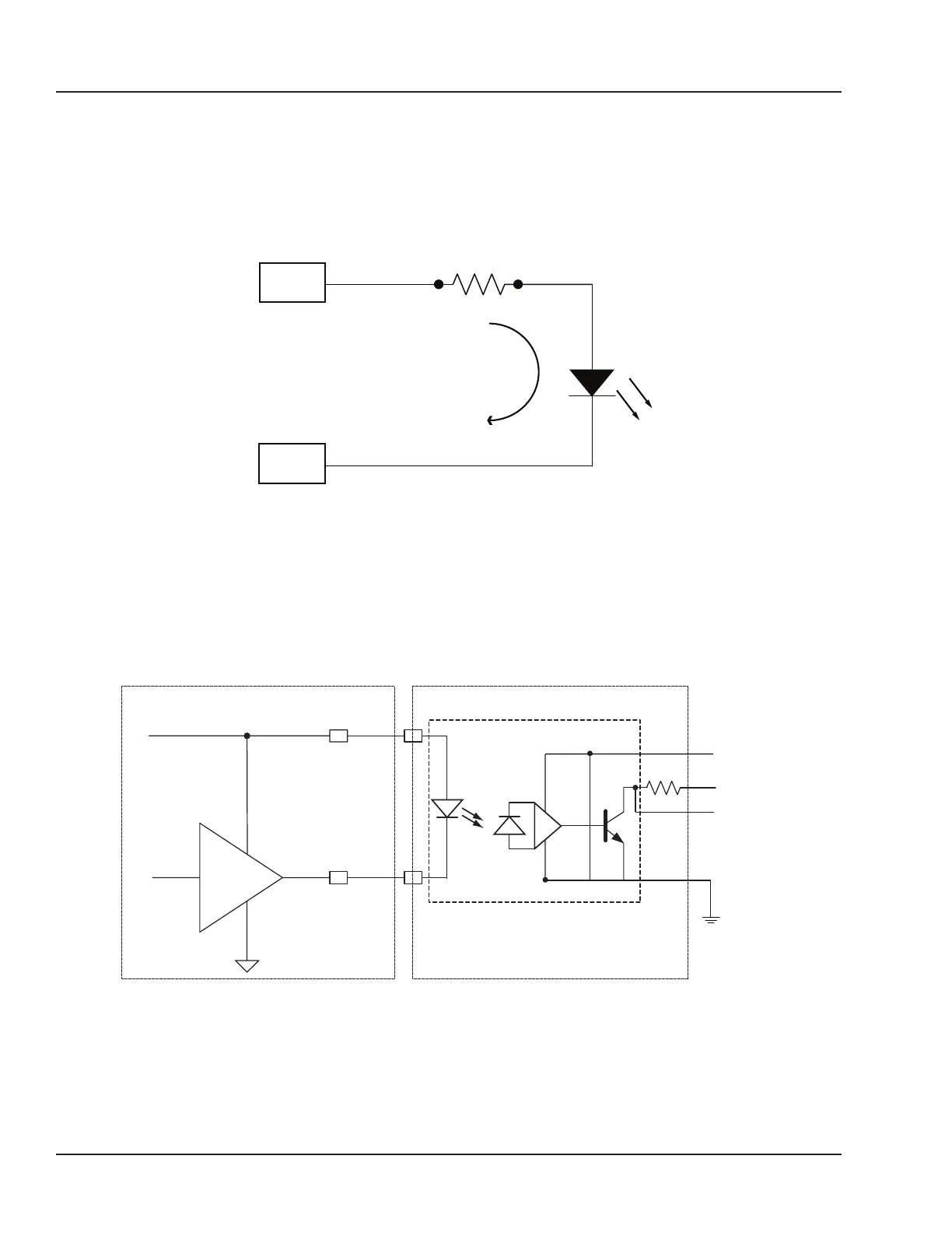
OP4250-1 32 DIGITAL INPUTS
When current flows from Din + to Din -, the output of opto-coupler A is low and the Din_FPGA signal is
low.
When no current flows, the opto-coupler output A is high and the Din_FPGA signal is high.
The signal conditioning module inputs have both anode and cathode sides available to the user (on the
I/O connector).
MODE 1: COMMON ANODE
R
VUser
Din
I
Max. 10 mA
Figure 19: Both Din + and Din - are available to the user
TYPICAL APPLICATIONS
The diagrams below illustrate typical application examples.
TC4049/4050
Vcc
OPAL-RT Din
INTERFACE BETWEEN CMOS DRIVE AND OPAL-RT Din
+5V
User
+2.5V/+3.3V
FPGA
Figure 20: Typical digital input circuit