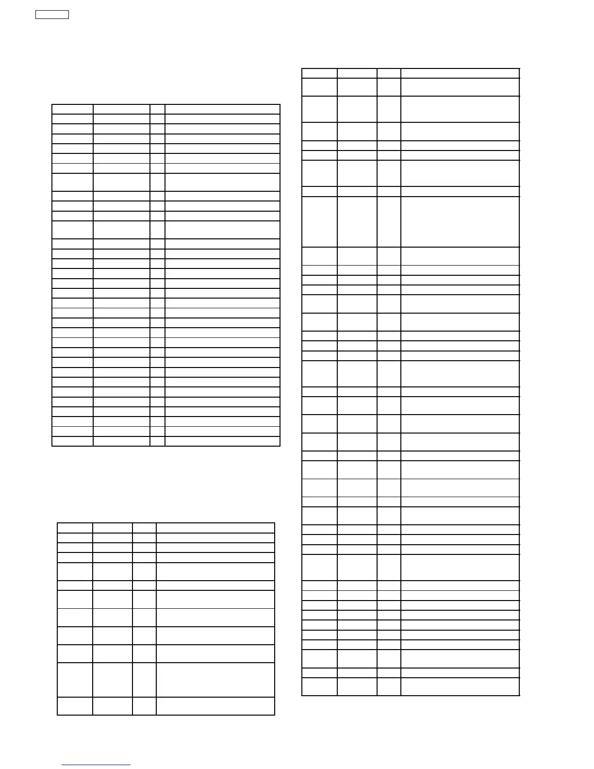
20.1. IC7001 (AN22004A-NF) Servo
Amplifier
Pin No. Mark I/O Function
1 LPD I Tracking signal input 1
2 LD I Tracking signal input 2
3 VCC - Power supply input
4 EQSW I Focus signal input terminal 1
5 RF I Focus signal input terminal 2
6 RFN I AGC amp input
7 CAGC O AGC loop Alter connecting
capacitor terminal
8 ARF O RF summing output
9 CEA I Detector’s input
10 ENV I 3TOUT output
11 DCDET I Capacitor for HPF amp
connection
12 CFTCONT I/O OFTR detect
13 BDO O BDO output (“H”: drop out)
14 OFTR O OFTR output
15 /RFDET O NRFDET output (“L” : detection)
16 LDON I LDON Terminal
17 GND - GND
18 EQBST -
19 VREF - VREF output Terminal
20 TEN I TE Amp Input (Low)
21 TEOUT - TE Amp output
22 FEN I FE Amp Input (Low)
23 FEOUT O FE Amp output
24 GCTL I/O GCTL Terminal
25 FBAL I/O Focus Balance control Terminal
26 TBAL TBAL control Terminal
27 PDE I Photo-diode Input
28 PDF I Photo-diode Input
29 D I
30 PDB I Photo-diode Input
31 C I
32 PDA I Photo-diode Input
20.2. IC7002 (MN662790RSC) Servo
Processor/ Digital Signal
Processor/ Digital Filter/ D/A
Converter
Pin No. Mark I/O Function
1 BCLK O Serial bit clock output
2 LRCK O L/R discriminating signal output
3 SRDATA O Serial data signal output
4 DVDD1 - Power supply input ( for digital
circuit)
5 DVSS1 - GND (digital circuit)
6 TX O Digital audio interface signal output
(Latches data at first transition)
7 MCLK I Microprocessor command clock
signal input
8 MDATA I Microprocessor command data
signal input
9 MLD I Microprocessor command load
signal input
10 SENSE O Sense signal output
(OFT,FESL,MAGEND,
NAJEND,POSAD,SFG)
(not used,open)
11 /FLOCK O Focus servo feeding signal output
(“L” : Feed)
Pin No. Mark I/O Function
12 /TLOCK O Tracking servo feeding signal
output (“L” : Feed)
13 BLKCK O Sub-code block clock signal output
(BLKCKf = 75Hz during normal
playback)
14 SQCK I External clock signal input for sub-
code Q resistor
15 SUBQ I sub-code Q code output
16 DMUTE I Muting input (“H” : mute)
17 STAT O Status signal output
(CRC,CUE,CLVS,TTSTVP,
FCLV,SQCK)
18 /RST I Reset signal input
19 SMCK - 1/2-diveded clock signal of crystal
osscillating at MSEL = “H” (SMCK
= 8.4672 MHz) 1/4 divided clock
signal of crystal oscillating at
MSEL = :L: (fSMCK = 4.2336MHz)
(Not connected, open)
20 CSEL I Frequency Selection Terminal H =
33.8688 MHz ; L = 16.9344MHz
21 TRV - (Not connected, open)
22 TVD O Traverse drive output
23 PC O Spindle motor ON output (“L” : N)
24 ECM O Spindle motor drive signal output
(focred mode output)
25 ECS O Spindle motor drive signal output
(servo error signal output)
26 KICK - (Not connected, open)
27 TRD O Tracking drive output
28 FOD O Focus drive output
29 VREF I D/A (drive) output (TVD, ECS,
TRD, FOD, FBAL, TBAL
Reference voltage input
30 FBAL O Focus balance adjustment output
31 TBAL O Tracking balance adjustment
output
32 FE I Focus error signal input (analog
input)
33 TE I Tracking error signal input (analog
input)
34 RFENV I RF envelope signal input
35 VDET I Vibration detection signal input (“H”
;detection)
36 OFT I Off-track signal input (“H” : off
track)
37 TRCRS I Track cross signal input
38 /RFDET I RF detection signal input (“L” :
detection)
39 BDO I Dropout signal input (“H” : Dropout)
40 LDON O Laser on signal output (“H” : ON)
41 PLLF2 - (Not connected, open)
42 DSLF2 O Tracking Offset alignment
output/DSL Balance Output (DA
Output)
43 WVEL O
44 ARF I RF signal input
45 IREF I Reference current input
46 DRF I DSL bias terminal (not used, open)
47 DSLF I/O DSL loop filter terminal
48 PLLF I/O PLL loop filter terminal
49 VCOF I/O VCO loop filter terminal
50 AVDD2 - Power supply input (for analog
circuit)
51 AVSS2 - GND (for analog circuit)
52 EFM - FM signal output (Not connected,
open)
20 Terminal Function of IC’s
90
SA-VK31EE