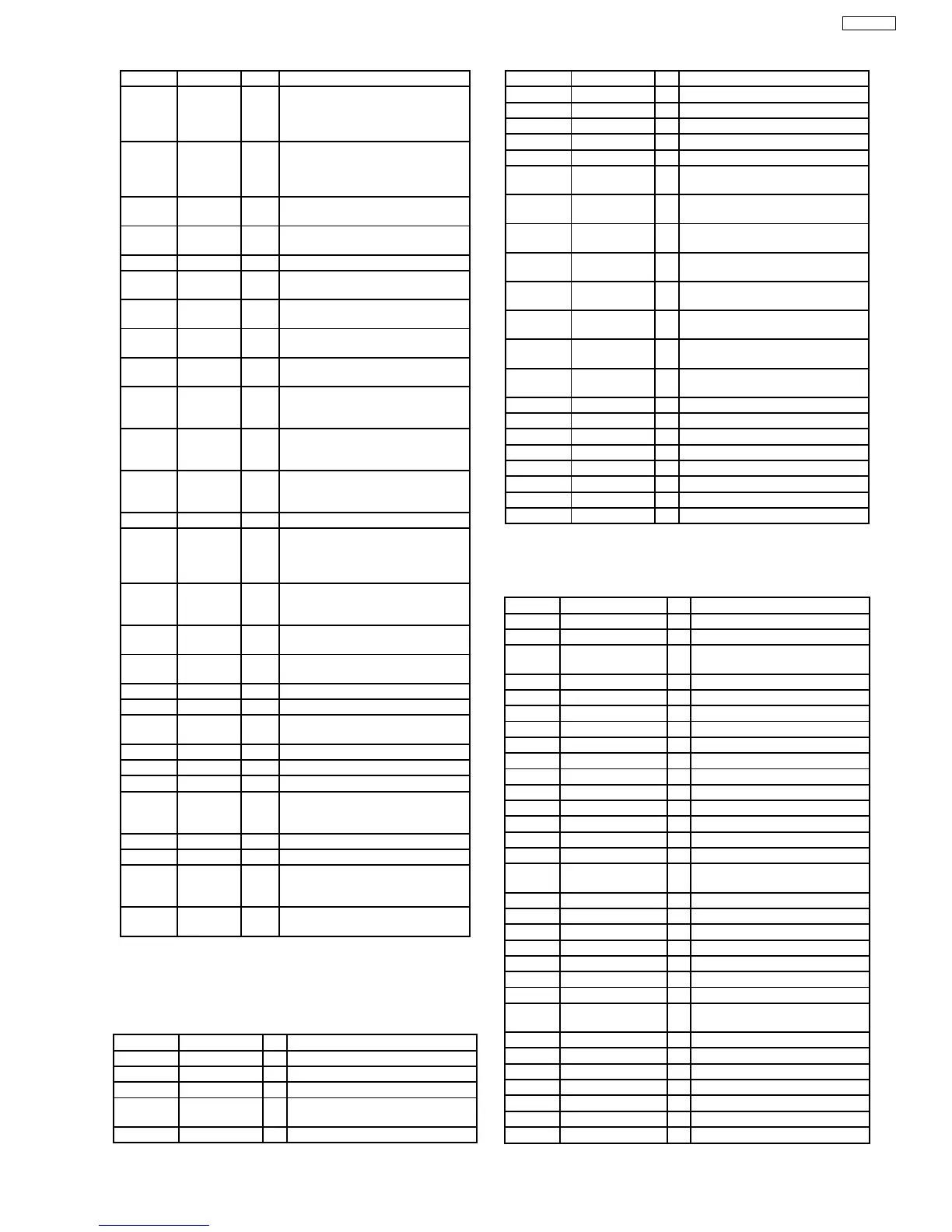
Pin No. Mark I/O Function
53 PCK - PLL extraction clock output (fPCK
= 4.321 MHz during normal
playback)
(Not connected, open)
54 VCOF2 I/O VCO Loop filter for 33.8688MHz
conversation terminaal for 16.9344
MHz crystal mode, must use other
circuit
55 SUBC - Sub-code serial data output (Not
connected, open)
56 SBCK I Clock input for sub-code serial
data
57 VSS - GND
58 X1 IN I Crystal oscillating circuit input (f =
16.9344MHz)
59 X2 OUT O Crystal oscillating circuit input ( f =
16.9344MHz)
60 VDD - Power supply input ( for oscillating
circuit)
61 BYTCK - Byte clock output (Not connected,
open)
62 /CLDCK - Sub-code frame clock signal output
(fCLDCK = 7.35 kHz during normal
playback)
63 FCLK - Crystal frame clock signal output
(fCLK = 7.35 kHz, double = 14.7
kHz)
64 IPFLAG - Interpolation flag output (“H” :
Interpolation) (Not connected,
open)
65 FLAG - Flag output (Not connected, open)
66 CLVS - Spindle servo phase synchronizing
signal output (“H” : CLV, “L” :
rough servo) (Not connected,
open)
67 CRC - Sub-code CRC checked output
(“H” :OK, “L”:NG) (Not connected,
open)
68 DEMPH - De-emphassis ON signal output
(“H” :ON) (Not connected, open)
69 RESV - Frame re-synchronizing signal
output (Not connected, open)
70 IOSEL I/O Mode Switching Terminal
71 /TEST I Test input
72 AVDD1 I Power supply input (for analog
circuit)
73 OUTL I Left channel audio signal output
74 AVSS1 I GND
75 OUTR O Right channel audio signal output
76 RSEL I RF signal polarity assignment input
(at “H” level, RSEL=”H”, at “L”
level, RESL = “L”)
77 IOVDD I 5V supply input
78 DIDATA I Test terminal (connected to Gnd)
79 DILRCK I SMCK osillating frequency
designation input (“L”:4.2336 MHz,
“H”:8.4672 MHz)
80 DISCK I SUBQ output mode select (“H”:Q-
code buffer mode)
20.3. IC7003 (AN8739SBTE2) Focus
Coil/ Tracking Coil/ Traverse
Motor/ Spindle Motor Driver
Pin No. Mark I/O Function
1 /RST O RESET output terminal
2 NC - N.C.
3 IN2 I Motor drive (2) input
4 PC2 I Turntable motor drive signal (“L”
:ON)
5 NC - N.C.
Pin No. Mark I/O Function
6 IN1 I Motor driver (1) input
7 PVCC1 - N.C.
8 PGND1 - Power supply (1) for driver
9 PGND1 - Ground connection (1) for driver
10 D1- - N.C.
11 D1+ O Motor driver (1) reverse-action
output
12 D2- O Motor driver (1) forward-action
output
13 D2+ O Motor driver (2) reverse-action
output
14 D3- O Motor driver (2) forward-action
output
15 D3+ O Motor driver (3) reverse-action
output
16 D4- O Crystal oscillating circuit input (f =
16.9344MHz)
17 D4+ O Motor driver (4) reverse-action
output
18 NC O Motor driver (4) forward-action
output
19 PGND2 - N.C.
20 PVCC2 - Ground connection (2) for driver
21 VCC - Power supply (2) for driver
22 VREF - N.C.
23 IN4 - Power supply terminal
24 IN3 - Reference voltage input
25 RSTIN I Motor driver (4) input
26 NC I Motor driver (3) input
20.4. IC2801 (MN101C30AEB)
Mechacon IC
Pin No. Mark I/O Function
1 MX/UX - Not used (GND)
2-5 N.C. - Not used (GND)
6 VREF+ - A-D Converter + V reference
voltage
7 VDD - Power supply (+5V)
8 OSC2 I Oscillation Input
9 OSC1 I Oscillation Input
10 VSS - Analog Ground
11 VSS - Not used
12 XI - Not used
13 XO - Not used (GND)
14 MMOD - Not used (GND)
15 KCMND - Not used (GND)
16 FLAG - Not used (GND)
17 NC - Not used (GND)
18 SUBQ I CD Servo LSI sub-code data
19 SQCK O Clock for reading CD servo LSI
sub-code
20 ESS_RST O ESS Chip Reset
21 MICON_RST I Reset Input
22 CD_PCNT - Not used (GND)
23 EE_CS I/O EEPROM Chip Select
24 EE_DATA I/O EEPROM Data
25 EE_CLK I/O EEPROM Clock
26 /MCS - Not used (GND)
27 BLKCK I Block Clock used for reading
sub-code data
28 DC_DET - Not used (GND)
29-31 NC - Not used (GND)
32 DSA_STRB I/O Strobe line for DSA
33 DSA_DATA I/O Data line for DSA
34 DSA_CLK I/O Acknowledge line for DSA
35-48 N.C. - No connection
49 RESTSW I CD pickup head limit switch input
91
SA-VK31EE