PDP-507CMX
145
5678
56
7
8
C
D
F
A
B
E
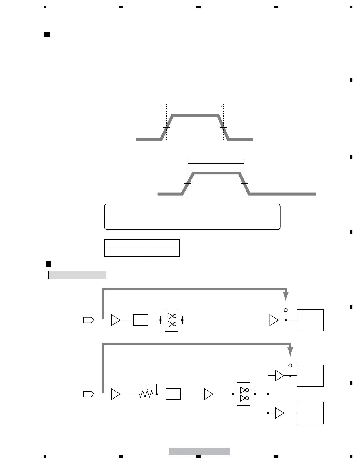
DELAY ADJUSTMENT OF THE CONTROL SIGNAL (SUS-D)
1 Measure the pulse width of the SUS-D signal.
2 Check the pulse width of the SUS-D input signal for the DK module.
Adjust the variable control so that the pulse width of the SUS-D input signal for the DK module becomes the "pulse width of
the SUS-D signal ± 5 nsec."
Note: For details on measuring points of waveform, see the figure below.
50 % of the crest value 50 % of the crest value
50 % of the crest value 50 % of the crest value
SUS-D pulse width: Tsus-Dg
Adjust so that "Tsus-Dg = Tsus-D ± 5 nsec," using the variable
control shown in the table below:
SUS-D signal (input to the DRIVE Assy)
SUS-D signal (input to the DK module)
SUS-D pulse width
Tsus-D
SUS-D pulse width
Tsus-Dg
Assy VR
Y MAIN DRIVE VR2002
SUS-B ADJUSTMENT
X DRIVE Assy
XSUS-U
from
DIGITAL Assy
IC1001_A2
Pin
3
Pin
2
Pin 2
IC1102
IC1205
IC1101
IC1104
X DK
Module
Q1102
TP1106
Photo
Coupler
1 Measure the SUS-B SUS-U input delay time (∆ Tsus-u).
from
DIGITAL Assy
XSUS-B
IC1001_A1
VR1001
Q1210
FET
Q1211
FET
Photo
Coupler
IC1204
Q1213
Q1209
TP1260
2 Adjust the SUS-B input delay time so that it becomes "∆ Tsus-u + α ± 5 nsec."
 Loading...