10 Operational Specifications
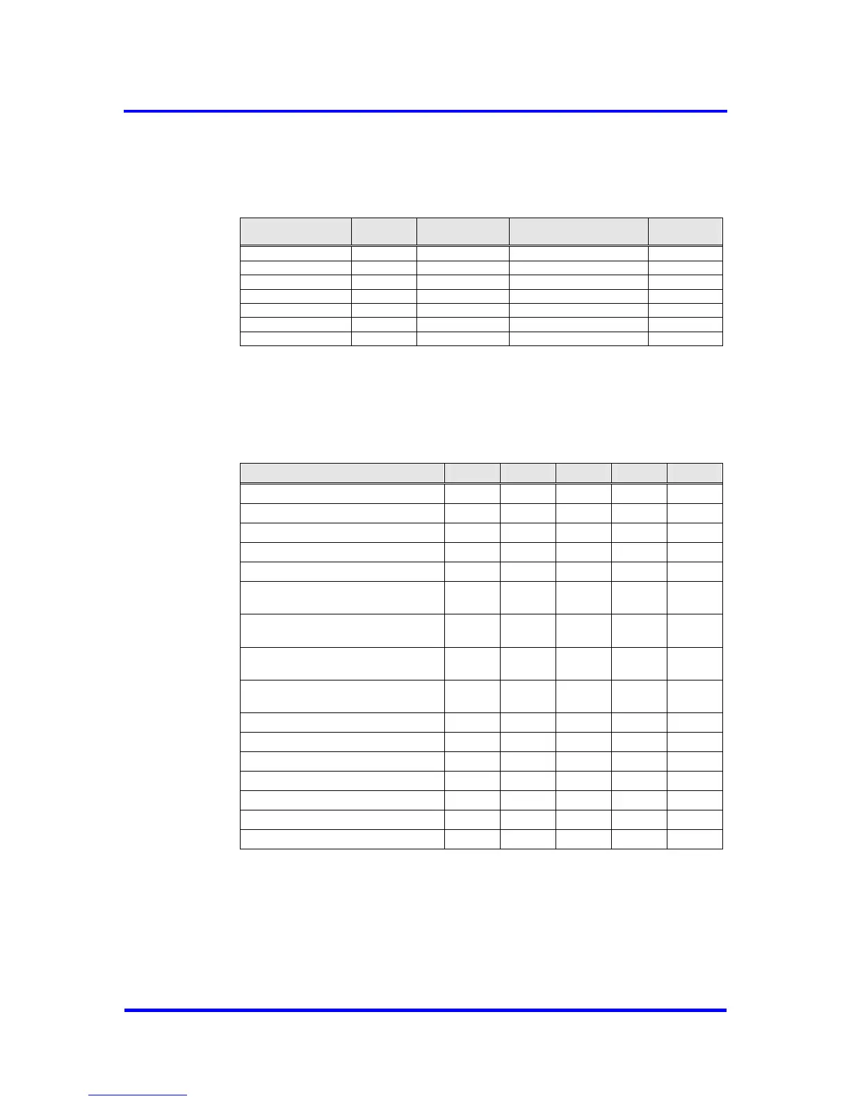
10.4 Ratings for the Output Drivers
Signal Direction
Driver
Ty pe
Driver gth Stren
Max. Cap.
Load
DB 0-7 I/O Tristate 8 100pF mA
RTS O Pus l 8m 50ph/Pul A F
TXD O Tristate 8m 50pA F
X/INT O Push/Pull 4mA 50pF
XREADY/XDTACK O Push/Pull 4mA 50pF
XDATAEXCH O Push/Pull 8mA 50pF
CLKOUT2/4 O Push/Pull 8mA 100pF
Figure 10-4: Ratings for the Output Drive
10.5 DC Electrical Characteristics Specification for 5V Operation
rs
Parameter Sy ol MIN TYP M mb AX Unit
DC supply voltage V
DD
4.50 5.00 5.50 V
CMOS input voltage LOW level 0.3 V
ILC
0 V
DD
V
CMOS input voltage HIGH level V
IHC
0 V.7 V
DD
DD
V
Output voltage LOW level V
OL
0 .4 V
Output voltage HIGH level V
OH
3.5 V
CMOS Schmitt Trigger
negative going threshold voltage
1
V
T-
1.5 .8 V
CMOS Schmitt Trigger
V
3.2
positive going threshold voltage
T+
3.5 V
TTL Schmitt Trigger
going threshold voltage
V
T-
0.9 1.1 V
negative
TTL Schmitt Trigger
positive going threshold voltage
V
T+
1.9 2.1 V
Input LOW current I
IL
-1 +1 µA
Input HIGH current I
IH
-1 +1 µA
Tri-state leakage current I
OZ
-10 ±1 +10 µA
Output current LOW level, 4mA cell I
OL
4.0 mA
Output current HIGH level, 4mA cell I
OH
-4.0 mA
Output current LOW level, 8mA cell I
OL
8.0 mA
Output current HIGH level, 8mA cell I
OH
-8.0 mA
Figure 10-5: DC Specification of I/O Drivers for 5V Operation
82 Revision 1.03
VPC3+C
User Manual
Copyright © profichip GmbH 2004-2006

 Loading...