Memory Organization 4
4.2 Control Parameters (Latches/Registers)
These cells can be either read-only or write-only. In the Motorola Mode the
VPC3+C carries out ‘address swapping’ for an access to the address
locations 00H - 07H (word registers). That is, the VPC3+C internally
generates an even address from an odd address and vice-versa.
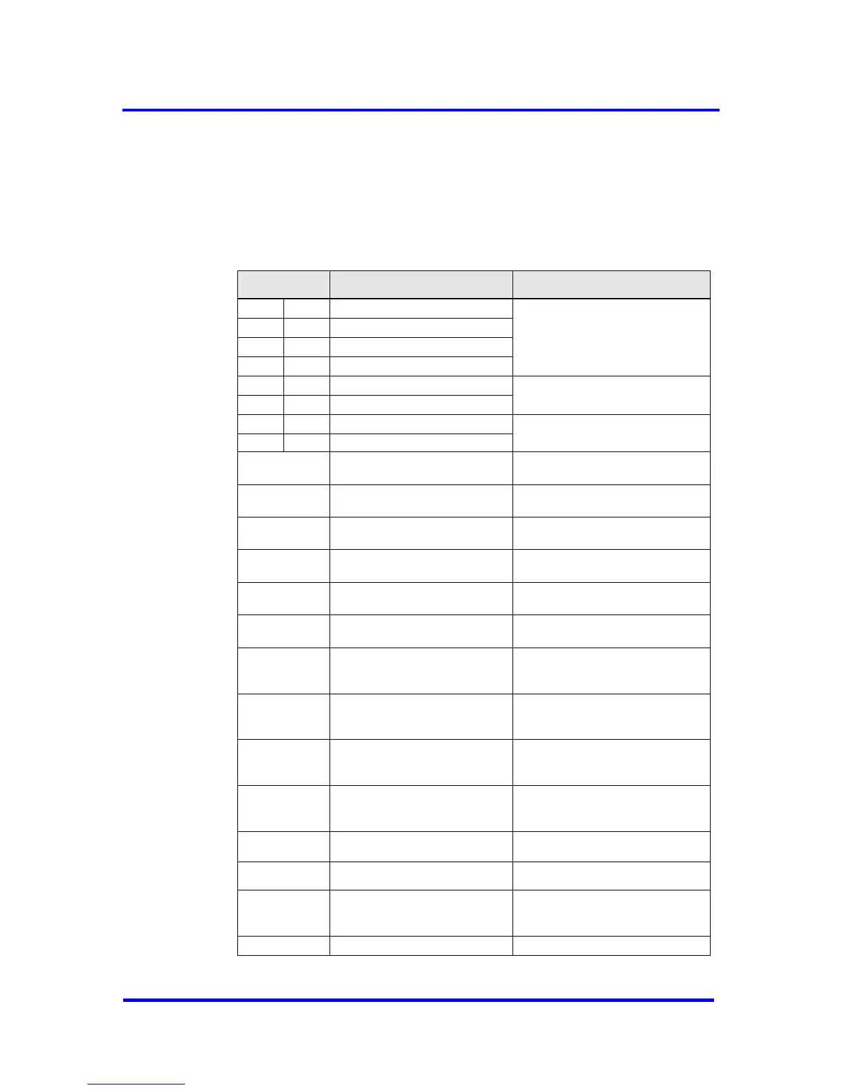
Address
Intel Mot. Name Bit No. Significance (Read Access!)
00H 01H
Int-Req-Reg 7..0
01H 00H
Int-Req-Reg 15..8
02H 03H
Int−Reg 7..0
03H 02H
Int−Reg 15..8
Interrupt Controller Register
04H 05H
Status-Reg 7..0
05H 04H
Status-Reg 15..8
Status Register
06H 07H
Mode-Reg 0 7..0
07H 06H
Mode-Reg 0 15..8
Mode Register 0
08H Din_Buffer_SM 7..0
Buffer assignment of the
DP_Din_Buffer_State_Machine
09H New_Din_Buffer_Cmd 1..0
The user makes a new DP Din_Buf
available in the N state.
0AH Dout_Buffer_SM 7..0
Buffer assignment of the
DP_Dout_Buffer_State_Machine
0BH Next_Dout_Buffer_Cmd 3..0
The user fetches the last DP
Dout_Buf from the N state
0CH Diag_Buffer_SM 3..0
Buffer assignment for the
DP_Diag_Buffer_State_Machine
0DH New_Diag_Buffer_Cmd 1..0
The user makes a new DP
Diag_Buf available to the VPC3+C.
0EH User_Prm_Data_Okay 1..0
The user positively acknowledges
the user parameter setting data of a
Set_(Ext_)Prm telegram.
0FH User_Prm_Data_Not_Okay 1..0
The user negatively acknowledges
the user parameter setting data of a
Set_(Ext_)Prm telegram.
10H User_Cfg_Data_Okay 1..0
The user positively acknowledges
the configuration data of a Chk_Cfg
telegram.
11H User_Cfg_Data_Not_Okay 1..0
The user negatively acknowledges
the configuration data of a Chk_Cfg
telegram.
12H
DXBout_Buffer_SM 7..0
Buffer assignment of the
DXBout_Buffer_State_Machine
13H
Next_DXBout_Buffer_Cmd 2..0
The user fetches the last
DXBout Buf from the N state
14H SSA_Buffer_Free_Cmd
The user has fetched the data from
the SSA_Buf and enables the buffer
again.
15H
Mode-Reg 1 7..0
Figure 4-2: Assignment of the Internal Parameter-Latches for READ
VPC3+C User Manual
Revision 1.03 15
Copyright © profichip GmbH 2004-2006