Operational Specifications 10
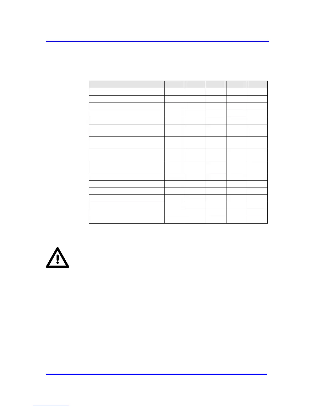
10.6 DC Electrical Characteristics Specification for 3.3V Operation
Parameter Symbol MIN TYP MAX Unit
DC supply voltage V
DD
3.00 3.30 3.60 V
CMOS input voltage LOW level V
ILC
0 0.3 V
DD
V
CMOS input voltage HIGH level V
IHC
0.7 V
DD
5.50 V
Output voltage LOW level V
OL
0.4 V
Output voltage HIGH level V
OH
2.4 V
CMOS Schmitt Trigger
negative going threshold voltage
V
T-
0.8 V
CMOS Schmitt Trigger
positive going threshold voltage
V
T+
2.7 V
TTL Schmitt Trigger
d voltage
V
T-
0.6 V
negative going threshol
TTL Schmitt Trigger
ld voltage
V
T+
1 V
positive going thresho
.7
Input LOW current I
IL
-1 +1 µA
Input HIGH current I
IH
-1 +1 µA
Tri-state leakage current I
OZ
-10 ±1 +10 µA
Output current LOW level, 4mA cell I
OL
+2.8 mA
Output current HIGH level, 4mA cell I
OH
-2.8 mA
Output current LOW level, 8mA cell I
OL
+5.6 mA
Output current HIGH level, 8mA cell I
OH
-5.6 mA
Figure 10-6: DC Specification of I/O Drivers for 3.3V Operation
N
For 3.3V operation the VPC3+C is equipped with 5V tolerant inputs except
f
t
or 3.3V operation the guaranteed minimum output current is 70% of that
otes:
or the clock pin CLK. When using 3.3V supply voltage the clock input needs
o be 3.3V level.
F
for 5V operation mode.
VPC3+C User Manual
Revision 1.03 83
Copyright © profichip GmbH 2004-2006