Operational Specifications 10
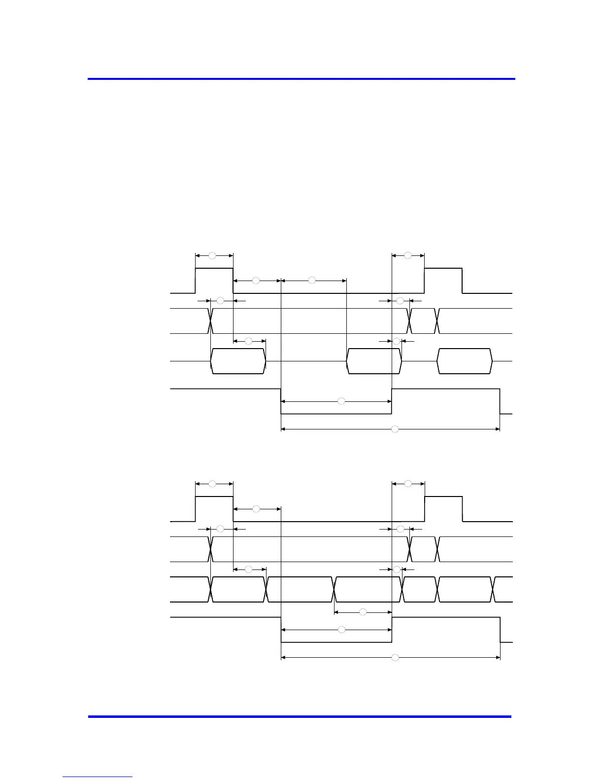
10 .2 the Synchronous Intel Mode
he synchronous Intel mode, 3+C latches the least significant
ith the falling edge
icant address bits on the address bus. An inter
al is generated from the most significant addre s bits e
t for an access to the VPC3+C is generated from the fa g ed of
read signal (XRD) and from the rising edge of the write signal (XWR).
.7 Timing in
In t the VPC
addresses w
expects the most signif
of ALE. At the same time, the VPC3+C
nal
. Thchipselect sign s
reques llin ge
the
ALE
AB10..0
DB7..0
XRD
valid
va d
data valid
address
address
li
1
2
3
4
5
6
10
9
8
7
Figure 10-9: Synchronous Intel Mode, READ (XWR = 1)
ALE
AB10..0
DB7..0
XWR
valid
valid
data valid
address
address
1
11
3
15
13
12
10
15
8
14
Figure 10-10: Synchronous Intel Mode, WRITE (XRD = 1)
VPC3+C User Manual
Revision 1.03 85
Copyright © profichip GmbH 2004-2006