Renesas RA Family MCK-RA6T2 User's Manual
R12UZ0091EJ0100 Rev 1.00 Page 23 of 38
August 3, 2021
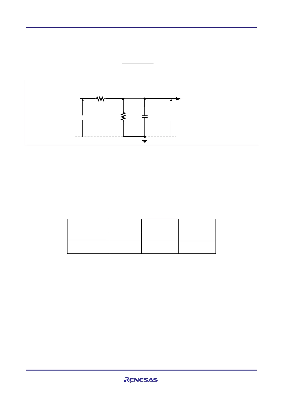
5.1.4 Output voltage detection circuit
The INV-BRD has the circuit that inputs bus voltage and three-phase output voltage (U, V and W phase) into
the AD pin of the microcontroller through resistive voltage divider. Relation between the three-phase output
voltage, the bus voltage and the detection voltage is described by the below equation (3).
Figure 5-4 Output voltage detection circuit
5.1.5 Voltage generation circuit
On the INV-BRD, the gate driver voltage ("+12V" in the schematic) is generated from the 5V power supply
("+5V" in the schematic) with the boost converter. If 5V is not supplied from the CPU board, the buck
converter on the INV-BRD generates 5V from the voltage input (12 to 48V) from the DC jack or terminal
block.
Table 5-1 Voltage generation

 Loading...


