TPS-1 User’s Manual: Hardware 8. PROFINET IO switch
R19UH0081ED0107 Rev. 1.07 page 55 of 86
Jul 30, 2018
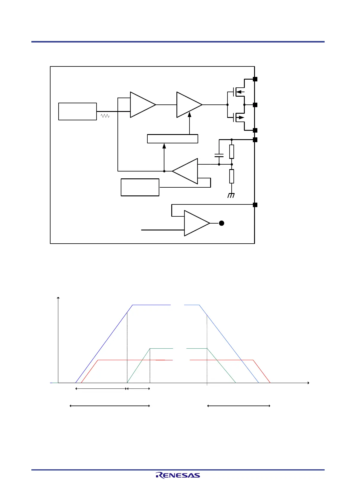
It is important that the input FB is connected to a smoothed 1.5 V voltage. The regulator adjusts the output voltage with negative feedback using this
pin.
BVDD (3.3 V Chip Supply)
Pin J1
-
+
-
+
Over Current Protection
PWM Comparator
Driver
LX (1.5 V Output)
Pin H1
AGND (BGND); Pin G1
FB (Feedback)
Pin F1
TPS-1
Band Gap
Reference Circuit
Triangle Wave
Generator
POR (chip internal use)
VREF
(internal)
AVDD_REG
(3.3 V Chip Supply)
Pin F2
Figure 8-2: Internal voltage regulator
The time of power-supply rise to the point where all power supplies are stabilized must be reached within 100 ms.
The typical behavior of the power supplies is shown in Figure 8-3: TPS-1 Power-up sequence.
Figure 8-3: TPS-1 Power-up sequence
T
rampup_3.3V
1.0V
2.0V
3.0V
T
rampup_1.5V
T
V
100ms 100ms
VDD
3.3V
VDD
1.5V
VDD
1.0V
 Loading...