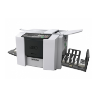
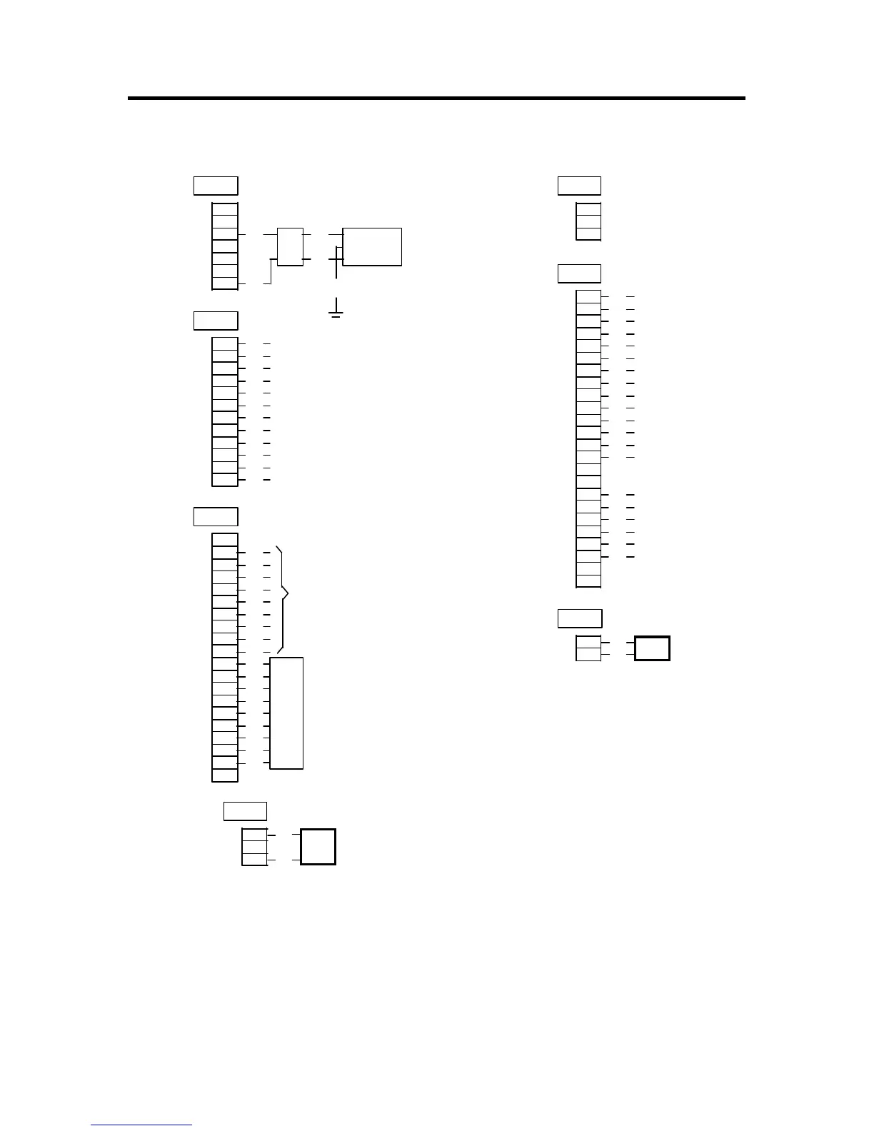
DESCRIPTION OF PCBs
POWER SUPPLY PCB 100-120V
APX(II)-27 GR3770
CN1
7pins
1
2
3
4
5
6
7
Bk
Wh
SW
Bk
Wh
Primary Power
W-H connector
Gr/Yw
AC
AC
CN2 12pins
1
2
3
4
5
6
7
8
9
10
11
12
+24VA (F3)
+24VC (F5)
+24VE (F7)
GND3
GNDM
+24VM (F2)
+24VB (F4)
+24VD (F6)
GNDD
GNDE
GNDM
+24VM (F2)
Or
Yw
Or
Br
Bk
Rd
Bl
Or
Br
Br
Bk
Rd
CN5-7 (System PCB2)
CN5-9 (System PCB2)
CN1-1 (Motor Control PCB MK2)
CN5-10 (System PCB2)
CN1-5 (Motor Control PCB MK2)
CN1-3 (Motor Control PCB MK2)
CN5-8 (System PCB2)
CN4-2 (Image Processing PCB)
CN4-1 (Image Processing PCB)
CN1-7 (Motor Control PCB MK2)
CN1-6 (Motor Control PCB MK2)
CN1-4 (Motor Control PCB MK2)
CN3-1
20pins
1
2
3
4
5
6
7
8
9
10
11
12
13
14
15
16
17
18
19
20
N.C.
GND2
GND2
GND2
GND2
GND2
GND2
GND2
GND2
GND2
+14V
+14V
+14V
+14V
+14V
+14V
+14V
+14V
+14V
N.C.
Br
Bl
Bl
Bl
Bl
Bl
Bl
Bl
Bl
Rd
Rd
Rd
Rd
Rd
Rd
Rd
Rd
Rd
TPH Safety switch
TPH Sub
PCB
LOW when activated
+24V (F7)
CN3-2
3pins
1
2
3
M
Suction fan
motor
Rd
Bl
CN4
3pins
1
2
3
CN5 24pins
1
2
3
4
5
6
7
8
9
10
11
12
13
14
15
16
17
18
19
20
21
22
23
24
+12V
+12V
GND1
-12V
TPH CTL
SUCTION CTL
PF/
PF/
GND1
GND1
GND1
GND1
GND1
GND1
GND1
GND1
+5.1V
+5.1V
+5.1V
+5.1V
+5.1V
+5.1V
+5.1V
+5.1V
Yw
Yw
Bk
Yw
Gr
Bl
Vt
Gy
Bk
Bk
Bl
Bk
Yw
Bk
Rd
Rd
Br
Rd
Bl
Rd
CN4-4 (Image Processing PCB)
CN5-3 (System PCB2)
CN4-3 (Image Processing PCB)
CN4-6 (LCD Control PCB)
CN5-4 (System PCB2)
CN5-5 (System PCB2)
CN4-7 (LCD Control PCB)
CN5-6 (System PCB2)
CN5-2 (System PCB2)
CN4-3 (LCD Control PCB)
CN4-4 (LCD Control PCB)
CN4-6 (Image Processing PCB)
CN4-5 (Image Processing PCB)
CN1-9 (Motor Control PCB MK2)
CN5-1 (System PCB2)
CN4-1 (LCD Control PCB)
CN4-2 (LCD Control PCB)
CN4-8 (Image Processing PCB)
CN4-7 (Image Processing PCB)
CN1-8 (Motor Control PCB MK2)
+24V (F7)
GND2
CN6
2pins
1
2
M
Power Supply
fan motor
Bk
Rd
Open