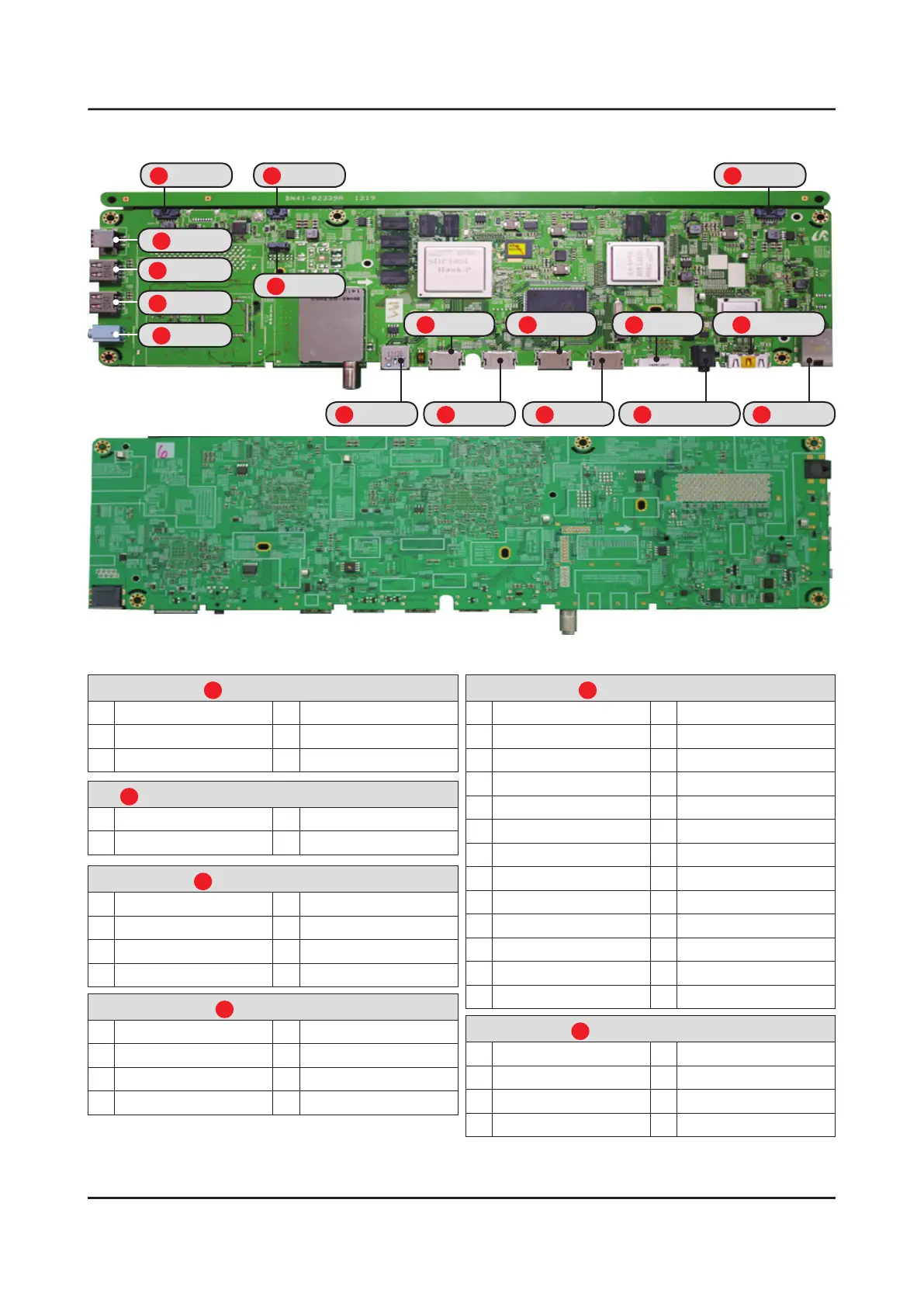
5-2-2. Jackpack Board (One connect)
12
CN2003
10
CN802
8
CN804
6
CN602_RS
4
CN1701
16
CN403
15
CN1803
14
CN1802
13
CN402
11
CN801
9
CN803
7
CN502
5
CN3301
1
CN2301
2
CN2102
17
CN501
3
CN1801
Jackpack Board (One connect) Pin Map
1
CN2301_DB (IRB)
1 A5V_PW 4 IRB_UART_TXD
2 SUB_RESET 5 DGND
3 IRB_UART_RXD 6 N.C
2
CN2102_DB (SUBMICOM SW DOWNLOAD)
1 DGND 3 DOWN_SDA_I2C
2 DOWN_SCL_I2C 4 DGND
3
CN1801 (ARM JTAG)
1 B3.3V_PW 5 FAN_ERROR
2 DGND 6 DGND
3 VOUT 7 VOUT
4 N.C 8 N.C
4
CN1701 (LAN)
1 MDI0_TX+_LAN 5 DGND
2 DGND 6 MDI1_RX-_LAN
3 MDI0_TX-_LAN 7 N.C
4 MDI1_RX+_LAN 8 LAN_GND
5
CN3301 (SERDES)
1 B3.3V_PW 14 SERDES_T2-
2 GCLK1_CLK 15 DGND
3 DGND 16 SERDES_T1+
4 SERDES_R1+ 17 SERDES_T1-
5 SERDES_R1- 18 DGND
6 DGND 19 SERDES_T5+
7 SERDES_T4+ 20 SERDES_T5-
8 SERDES_T4- 21 A5V_PW
9 DGND 22 RX_MICOM_JACK
10 SERDES_T3+ 23 TX_MICOM_JACK
11 SERDES_T3- 24 GCLK0_CLK
12 DGND 25 B13V_PW
13 SERDES_T2+ 26 B13V
6
CN602_RS (RS232C)
1 DGND 5 N.C
2 T1OUT 6 IDENT_FANET
3 R1IN 7 DGND
4 N.C

 Loading...