Pin No.
Signal
I/O
Description
10
D12
OUT
Similar to
D11
To indicate the first digit of Fluorescent Display.
11
813
OUT
Similar to
D11
To indicate the second digit of Fluorescent Display.
12
D14
OUT
Similar to
D11
To indicate the third digit of Fluorescent Display.
13
D15
OUT
Similar to Di
i
To indicate the fourth digit of Fluorescent Display.
14
VDISP
IN
Anode (segment) of Fluorescent Display light-up voltage: -25V.
Vp voltage of converter circuit is input.
15
RESET IN
Auto-clear terminal.
Signal is input to reset the LSI to the initial slate when power is supplied.
Temporarily set to “H” level the moment power is supplied, in this time the LSI is
reset.
Thereafter set “L” level
(-15V).
16
VBB
17
VDD
18
OSCl
IN
IN
IN
Power source voltage: -1 OV.
-10 volt of converter circuit is input.
Internal clock oscillation frequency setting input.
The internal clock frequency is set by inserting the ceramic filter oscillation circuit
with respect to
OS&
terminal.
19
OS&
OUT
Internal clock oscillation frequency control output.
Output to control oscillation input of
OSCl.
20
TEST
21
vss
22
ROO
23
ROl
24
Ro2
25
R03
26
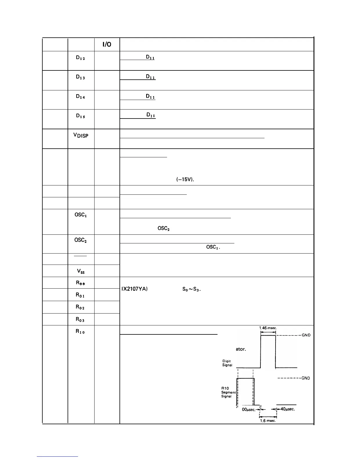
ho
IN
Terminal not used. Connected to GND.
IN
IN Input signal to be used for data supplying and reception with respect to LSI (l-l:
. IX2107YA) output signal:
So
-
Ss.
IN
IN
IN
OUT
Signal for lighting of power level indicators.
1.46
msec.
------_
-
GND
Normally signal similar Vp.
Pulse signals are generated when lighting either indicator.
Digit
Signal
IL
-30v
--------GN,,
0
1
OOpsec.+-
-25v
-i
p-40psec.
L
1.6
msec.
72