Posi‐
tion
Signal TiM3xx-01xxxx
(cable with flying
leads): wire color
TiM3xx-10xxxx (15-pin D-
Sub-HD male connector):
PIN
TiM3xx-11xxxx,
TiM3xx-21xxxx (12-pin
M12 male connector): PIN
X3 OUT 3 White 14 7
X4 OUT 4 Red + black 4 8
Y GND Black 5 1
OUT X 5
Y
Z
GND
X
V
S
2
V
S
V
out
3
Device 1
4
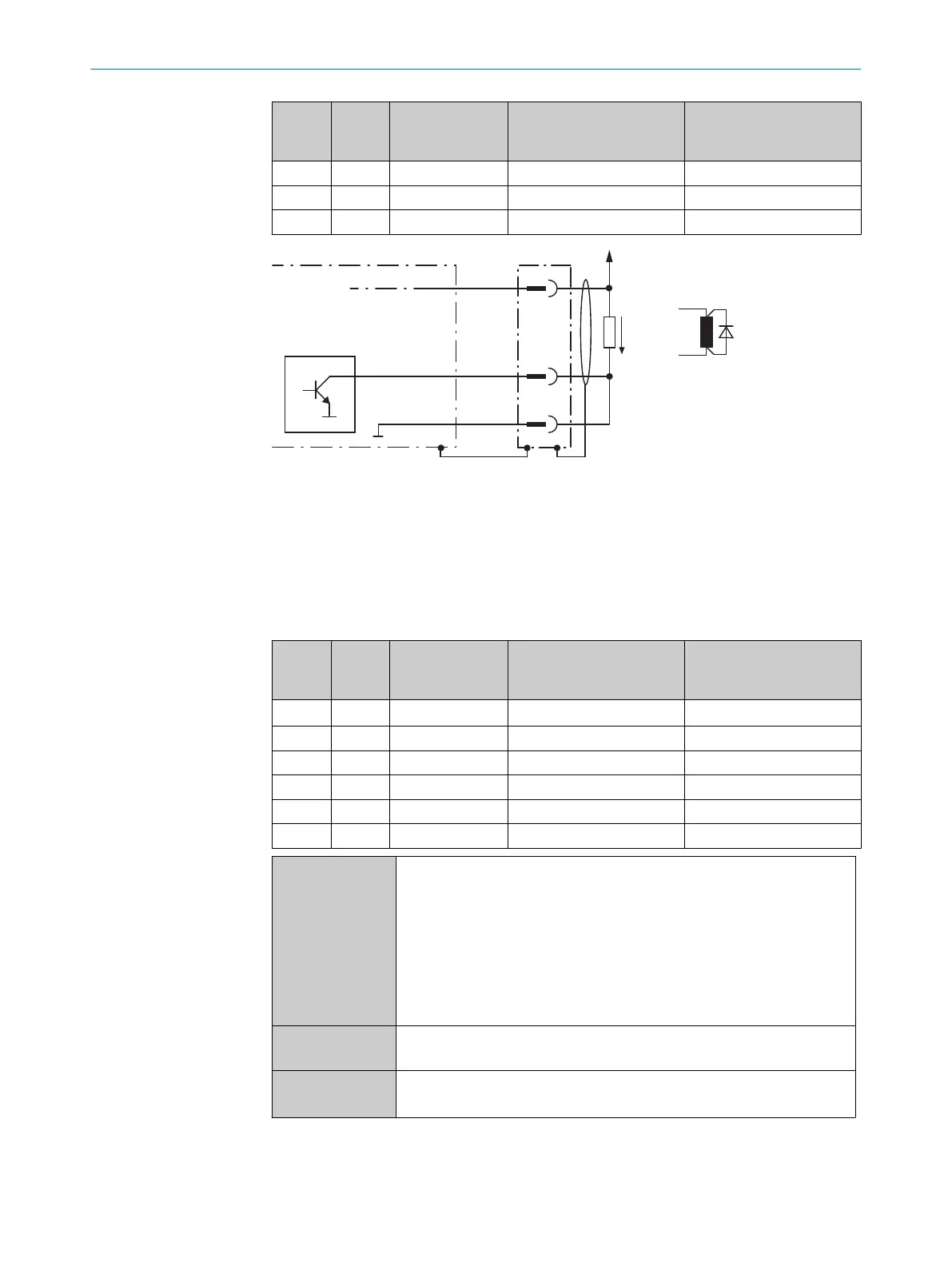
Figure 29: Wiring of digital output (NPN version)
1
Device
2
Supply voltage V
s
of the device
3
Output voltage V
out
4
If an inductive load is present: Provide an arc-suppression circuit at the digital switching
output. Attach a freewheeling diode directly to the load for this purpose.
5
Signal OUT X
Posi‐
tion
Signal TiM3xx-01xxxx
(cable with flying
leads): wire color
TiM3xx-10xxxx (15-pin D-
Sub-HD male connector):
PIN
TiM3xx-11xxxx,
TiM3xx-21xxxx (12-pin
M12 male connector): PIN
X V
S
Red 1 2
Y1 OUT 1 Brown 12 5
Y2 OUT 2 Orange 13 6
Y3 OUT 3 White 14 7
Y4 OUT 4 Red + black 4 8
Z GND Black 5 1
Switching behav‐
ior
PNP switching against supply voltage UV
OUT 1 ... OUT 3:
Resting level: High (no field breach), working level: Low (field breach)
Response time: 134 ms ... 30 s (configurable via SOPAS ET ), holding
time: 0 ms ... 10 s (configurable via SOPAS ET)
OUT 4:
Resting level: High (device ready)
working level: Low (error), low pulse (15 Hz, index, corresponds to meas‐
urement at 90°)
Properties Short-circuit protected and temperature protected
Not electrically isolated from supply voltage U
v
Electrical values 0 V ≤ V
out
≤ V
S
(V
S
– 1.5 V) ≤ V
out
≤ V
S
at I
out
≤ 100 mA
Longer connecting cables at the digital outputs of the device should be avoided due to
the resulting fall in voltage. This is calculated as follows:
Δ U = (2 x length x current) : (conductance value x cross-section)
ELECTRICAL INSTALLATION
6
8024851//2021-07-21 | SICK O P E R A T I N G I N S T R U C T I O N S | TiM3xx
39
Subject to change without notice