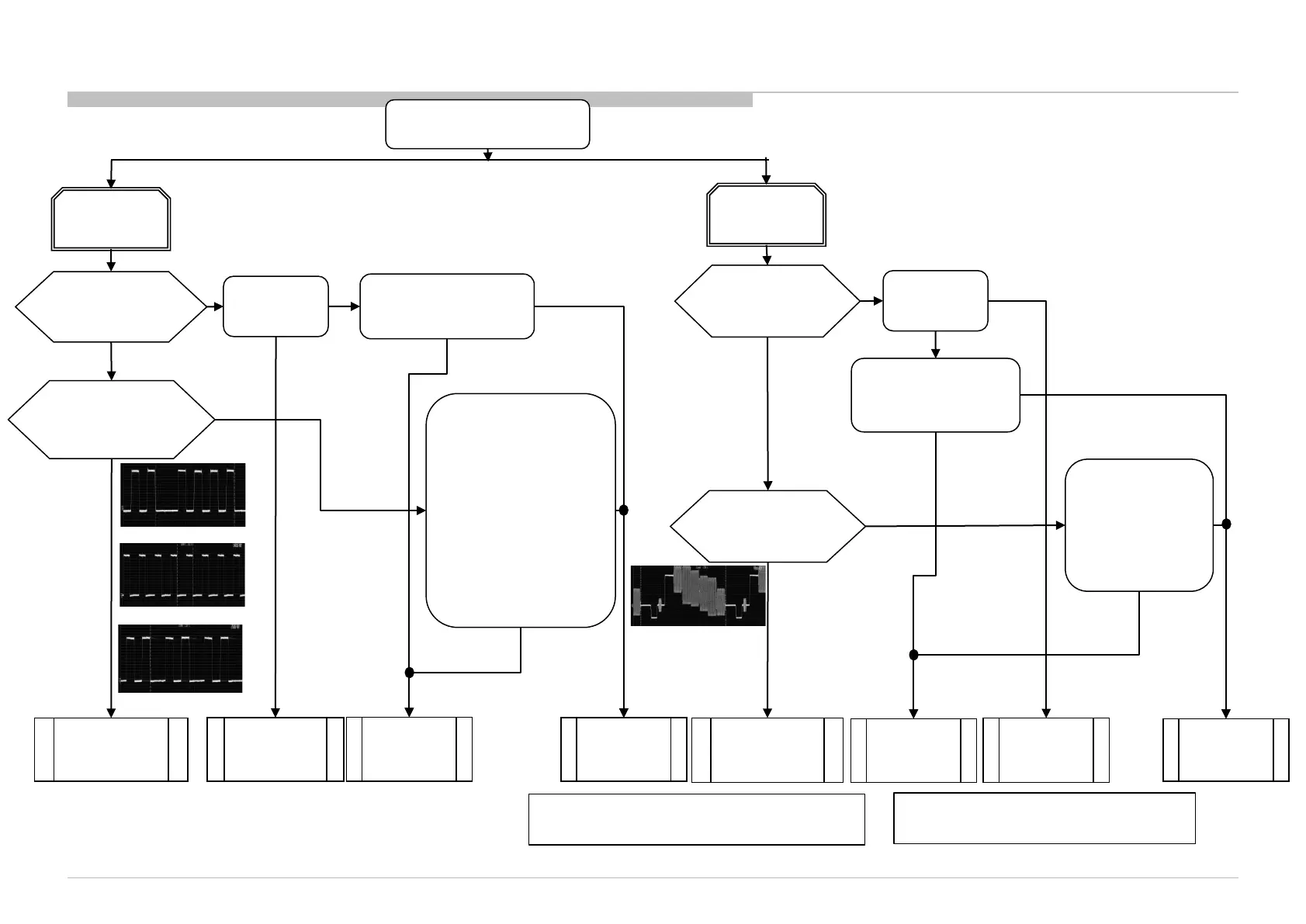
3f.9.3 Video Analog Signal Path – No Picture – General Checking - WW Destination (AEP/UK Only)
3f.9 Video Analog Signal Path
No Picture AEP/UK
SCART CVBS
No Picture
Check wave between
C3111 (Ref4)
and IC5000
Detailed check all
parts at CN3100 along
signal path at Pin No:
20 : [VD3107/R3107
/C3106/R3127]
Check RGB_SWITCH
IC5000 N25
[SOY1] at R3112
*Check CN3100
Connection
MT5581 [IC5000]
Problem
SCART RGB
No Picture
Check wave at
C3107(Ref1) /C3109(Ref2)
C3110(Ref3) & IC5000
** Detailed check all parts at
CN3100 along signal path
at Pin No:
7 : [VD3102/R3109/C3102/
R3123]
11 : [VD3103/R3110/C3103/
R3124]
15 : [VD3104/R3111/C3104/
R3125]
NG
(Vpp: 0V)
Check RGB_SWITCH
IC5000 N25
[SOY1] at R3112
*Check CN3100
Connection
NG
[LOW : 0V]
MT5581 [IC5000]
Problem
**Detailed check all parts
at RGB_SWITCH signal
Path [VD3105/R3105]
CN3100
Connectivity
Problem
Parts Broken
CN3100
Connector
Problem
OK
NG
CN3100
Connectivity
Problem
NG
OK
NG
NG
** Detailed check all parts
at RGB_SWITCH signal
Path [VD3105/R3105]
Parts Broken
CN3100
Connector
Problem
OK
OK
OK
NG
NG
OK
** OK Condition : No part short-circuited
NG Condition : Part short-circuited
NG
(Vpp: 0V)
OK
(Vpp: 1V)
* OK Condition : No solder splash can be seen
NG Condition : Solder splash can be seen
OK [HIGH: 3V RGB]
Ref4
Ref1
Ref2
Ref3
NG
[LOW : 0V]
OK
[HIGH: 0.4V]
OK
79