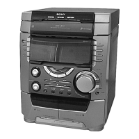
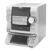
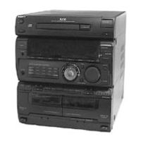
1313
SECTION 4
DIAGRAMS
4-1. NOTE FOR PRINTED WIRING BOARDS AND SCHEMATIC DIAGRAMS
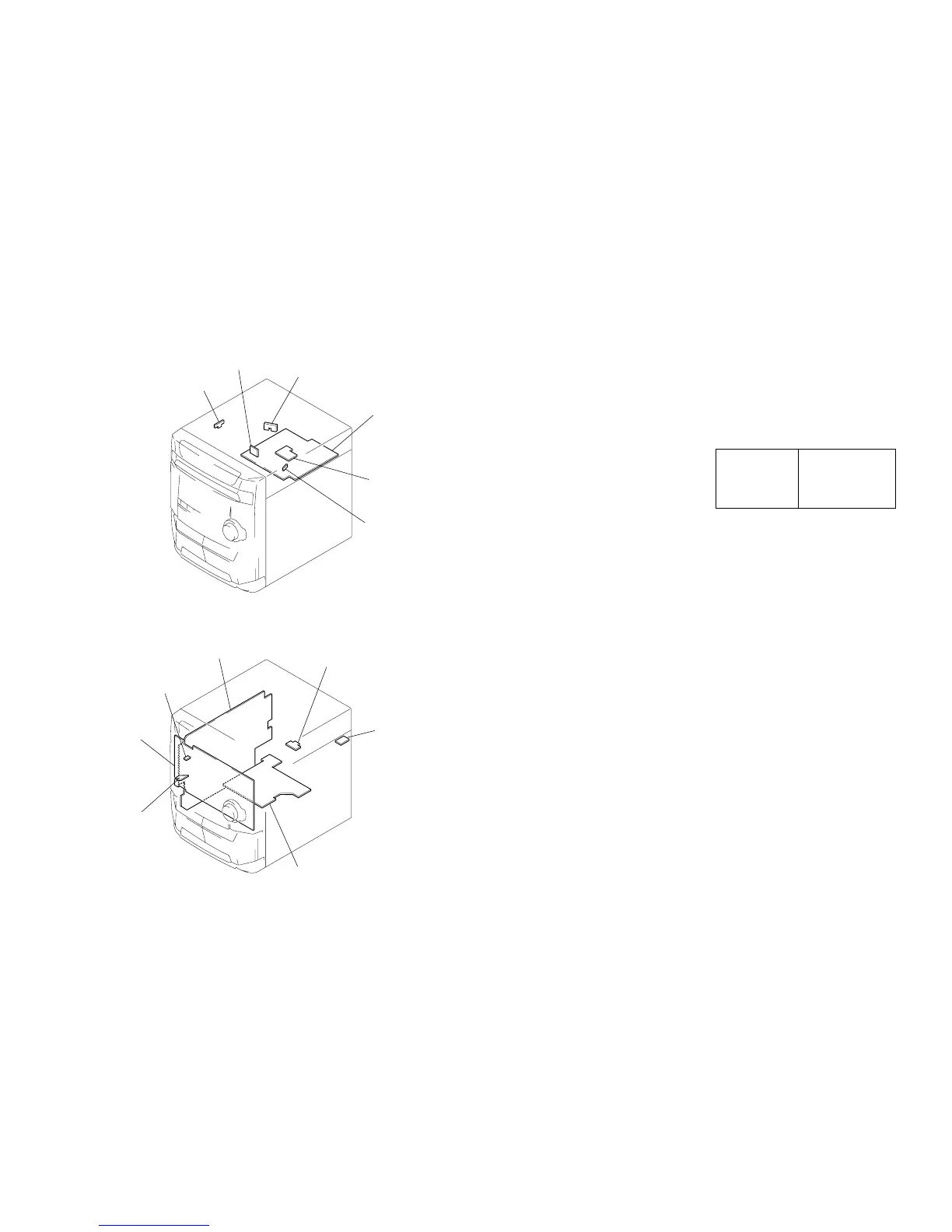
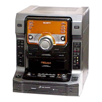
• Circuit Boards Location
Note on Printed Wiring Board:
• Y : parts extracted from the conductor side.
• b : Pattern from the side which enables seeing.
(The other layers' patterns are not indicated.)
Note on Schematic Diagram:
• All capacitors are in µF unless otherwise noted. U: µF,
pF: µµF 50 WV or less are not indicated except for
electrolytics and tantalums.
• If a numeric value of capacitor is a decimal fraction, the
preceding zero may be omitted.
(For example, .1 expresses 0.1)
• All resistors are in Ω and
1
/
4
W or less unless otherwise
specified.
• 5 : fusible resistor.
• 3 : printed resistor.
• C : panel designation.
• U : B+ Line.
• V : B– Line.
• H : adjustment for repair.
• Voltages are taken with a VOM (Input impedance 10 MΩ).
Voltage variations may be noted due to normal produc-
tion tolerances.
• Waveforms are taken with a oscilloscope.
Voltage variations may be noted due to normal produc-
tion tolerances.
• Circled numbers refer to waveforms.
• Signal path.
F : FM
f : AM
E : TAPE PLAY (DECK A)
d : TAPE PLAY (DECK B)
G : TAPE REC
J : CD PLAY (ANALOG OUT)
c : CD PLAY (DIGITAL OUT)
• Abbreviation
AUS : Australian model
CND : Canadian model
Note:
The components identi-
fied by mark 0 or dotted
line with mark 0 are criti-
cal for safety.
Replace only with part
number specified.
Note:
Les composants identifiés par
une marque 0 sont critiques
pour la sécurité.
Ne les remplacer que par une
pièce portant le numéro
spécifié.
SW C board
SW D board
SW B board
DECODE board
MOTOR boar