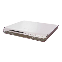
HCD-BX77DBi
HCD-BX77DBi
1919
For Schematic Diagrams.
Note:
• All capacitors are in μF unless otherwise noted. (p: pF) 50
WV or less are not indicated except for electrolytics and
tantalums.
• All resistors are in Ω and 1/4 W or less unless otherwise
specifi ed.
•
f
: Internal component.
• 2 : Nonfl ammable resistor.
• C : Panel designation.
THIS NOTE IS COMMON FOR PRINTED WIRING BOARDS AND SCHEMATIC DIAGRAMS.
(In addition to this, the necessary note is printed in each block.)
• A : B+ Line.
• B : B– Line.
• Voltages and waveforms are dc with respect to ground
under no-signal (detuned) conditions.
– CD board –
no mark
: CD PLAY
– DAB board –
no mark
: DAB
– IP board –
no mark
: iPod
– Other boards –
no mark
: TUNER (FM/AM)
( ) : CD PLAY
[ ] : iPod
< > : DAB
• Voltages are taken with VOM (Input impedance 10 MΩ).
Voltage variations may be noted due to normal production
tolerances.
• Waveforms are taken with a oscilloscope.
Voltage variations may be noted due to normal production
tolerances.
• Circled numbers refer to waveforms.
• Signal path.
F : AUDIO
f : TUNER (FM/AM)
J : CD PLAY
O : iPod
L : DAB
h : AUDIO IN
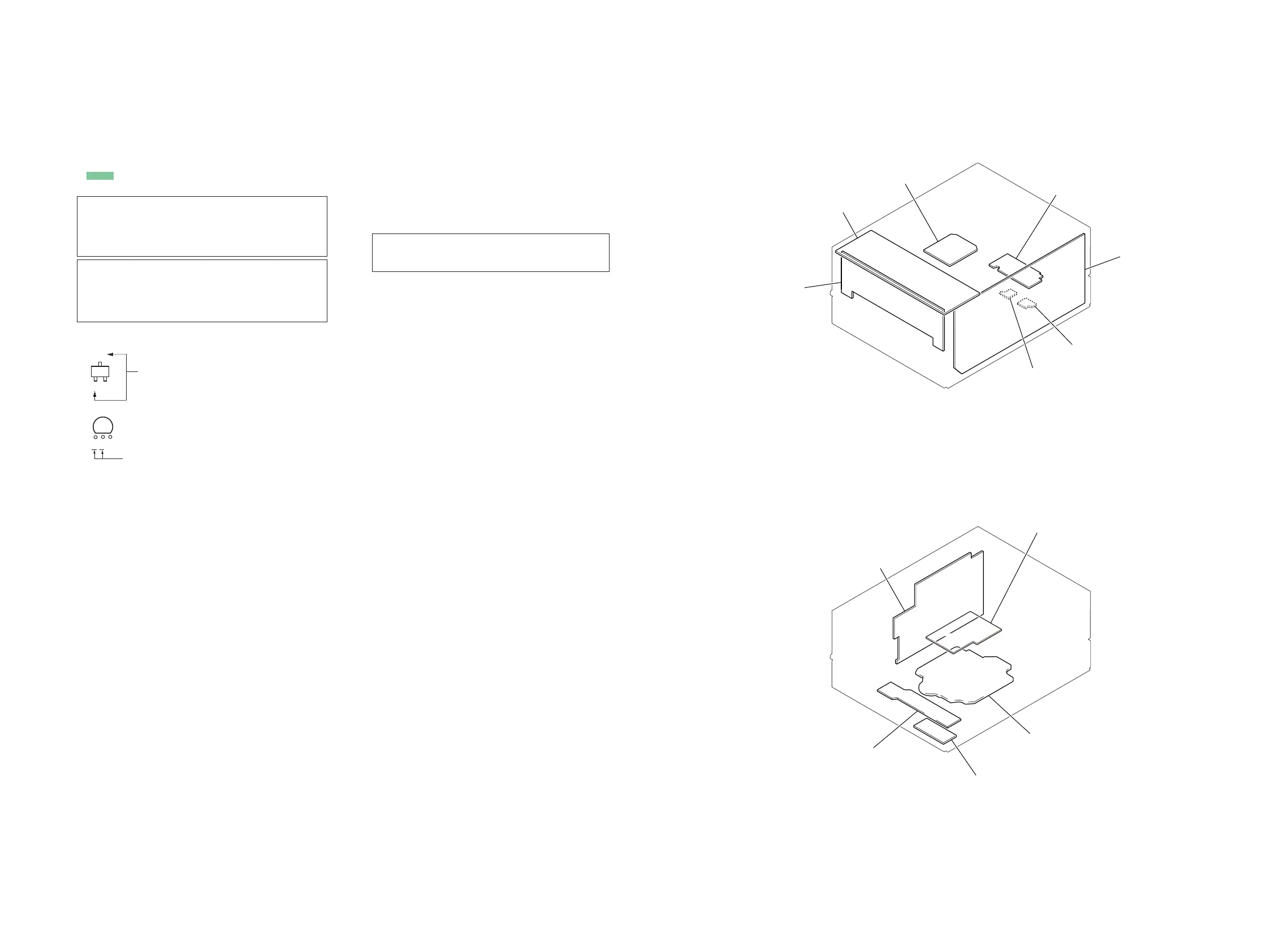
For Printed Wiring Boards.
Note:
• X : Parts extracted from the component side.
• Y : Parts extracted from the conductor side.
•
f
: Internal component.
• : Pattern from the side which enables seeing.
(The other layers’ patterns are not indicated.)
• Indication of transistor.
These are omitted.
Caution:
Pattern face side:
(SIDE B)
Parts face side:
(SIDE A)
Parts on the pattern face side seen
from the pattern face are indicated.
Parts on the parts face side seen from
the parts face are indicated.
Note: The components identifi ed by mark 0 or dotted
line with mark 0 are critical for safety.
Replace only with part number specifi ed.
Caution:
Pattern face side:
(Conductor Side)
Parts face side:
(Component Side)
Parts on the pattern face side seen
from the pattern face are indicated.
Parts on the parts face side seen from
the parts face are indicated.