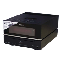
HCD-BX77DBi
42
Pin No. Pin Name I/O Description
62 VCC - Power supply terminal (+3.3V)
63 NC O Not used
64 VSS - Ground terminal
65 NC O Not used
66 I-POWER MONITOR I Power monitor input terminal
67 DEC BUS SEL O Bus selection signal output terminal Not used
68 MP3 IREQ I Request signal input from the CD-MP3 processor
69 CD CCE O Chip enable signal output to the CD-MP3 processor
70 CD CLK O Serial data transfer clock signal output to the CD-MP3 processor
71, 72 NC O Not used
73 NC I iPod connection detection signal input from the iPod connector “L”: iPod is connected
74 KEY WAKE UP I Wake up signal input terminal
75 USB RESET O Reset signal output terminal (for USB section) Not used
76 USB CTS I Clear to send signal input terminal (for USB section) Not used
77 CLINK-TX-DOUT O Serial data output to the iPod interface
78 CLINK-RX-DIN I Serial data input from the iPod interface
79 NC O Not used
80 DMPORT POWER O VBUS power on/off control signal output terminal “H”: power on
81 to 83 KEY3 to KEY1 I Top and front panel key input terminal (A/D input)
84 CDM LOAD OUT O Loading motor control signal output terminal (for loading out)
85 CDM LOAD IN O Loading motor control signal output terminal (for loading in)
86 SPEC IN I Setting terminal for the destination
87 CDM SW (OPEN) I Disc tray open position detection signal input terminal “L”: disc tray is opened
88 CDM SW (CLOSE) I Disc tray close position detection signal input terminal “L”: disc tray is closed
89 STANDBY LED O LED drive signal output terminal for STANDBY indicator “L”: LED on
90 FL RESET O Reset signal output to the fl uorescent indicator tube “L”: reset
91 FL CS O Chip select signal output to the fl uorescent indicator tube
92 FL SD O Serial data output to the fl uorescent indicator tube
93 FL SCLK O Serial data transfer clock signal output to the fl uorescent indicator tube
94 X5V FLAG I VBUS voltage detection signal input terminal
95 NC O Not used
96 AVSS - Ground terminal
95 NC O Not used
98 VREF I Reference voltage (+3.3V) input terminal
99 AVCC - Power supply terminal (+3.3V)
100 CD BUS3 O Serial data output to the CD-MP3 processor

 Loading...