30
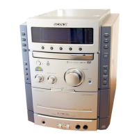
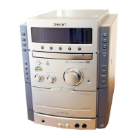
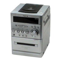
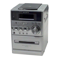
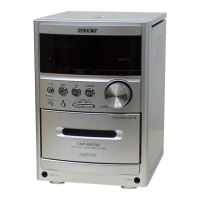
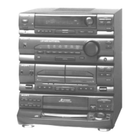
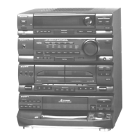
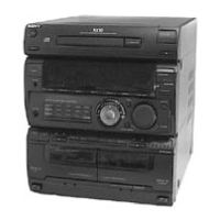
HCD-NXM2D
For schematic diagrams.
Note:
• All capacitors are in µF unless otherwise noted. (p: pF)
50 WV or less are not indicated except for electrolytics
and tantalums.
• All resistors are in Ω and
1
/
4
W or less unless otherwise
specified.
• f : internal component.
• 2 : nonflammable resistor.
• 5 : fusible resistor.
• C : panel designation.
• A : B+ Line.
• B : B– Line.
• H : adjustment for repair.
•Voltages and waveforms are dc with respect to ground
under no-signal conditions.
RF, DMB07, VIDEO boards section
no mark: DVD PLAY
Other board section
no mark: TUNER (FM/AM)
( ): DVD PLAY
< >: TAPE REC
[ ]: TAPE PLAY
* : Impossible to measure
•Voltages are taken with a VOM (Input impedance 10 MΩ).
Voltage variations may be noted due to normal produc-
tion tolerances.
•Waveforms are taken with a oscilloscope.
Voltage variations may be noted due to normal produc-
tion tolerances.
• Circled numbers refer to waveforms.
• Signal path.
F : TUNER (FM/AM)
E : TAPE PLAY (DECK A)
d : TAPE PLAY (DECK B)
G : RECORD
J : DVD PLAY
c : DVD PLAY (DIGITAL)
N : MIC INPUT
• Abbreviation
E2 : 120V AC Area in E model
E3 : 240V AC Area in E model
EA : Saudi Arabia mdoel
E15 : Iran model
SP : Shingapore model
MY : Malaysia model
TH : Thai model
Note: The components identified by mark 0 or dotted line
with mark ! are critical for safety.
Replace only with part number specified.
(The other layers' patterns are not indicated.)
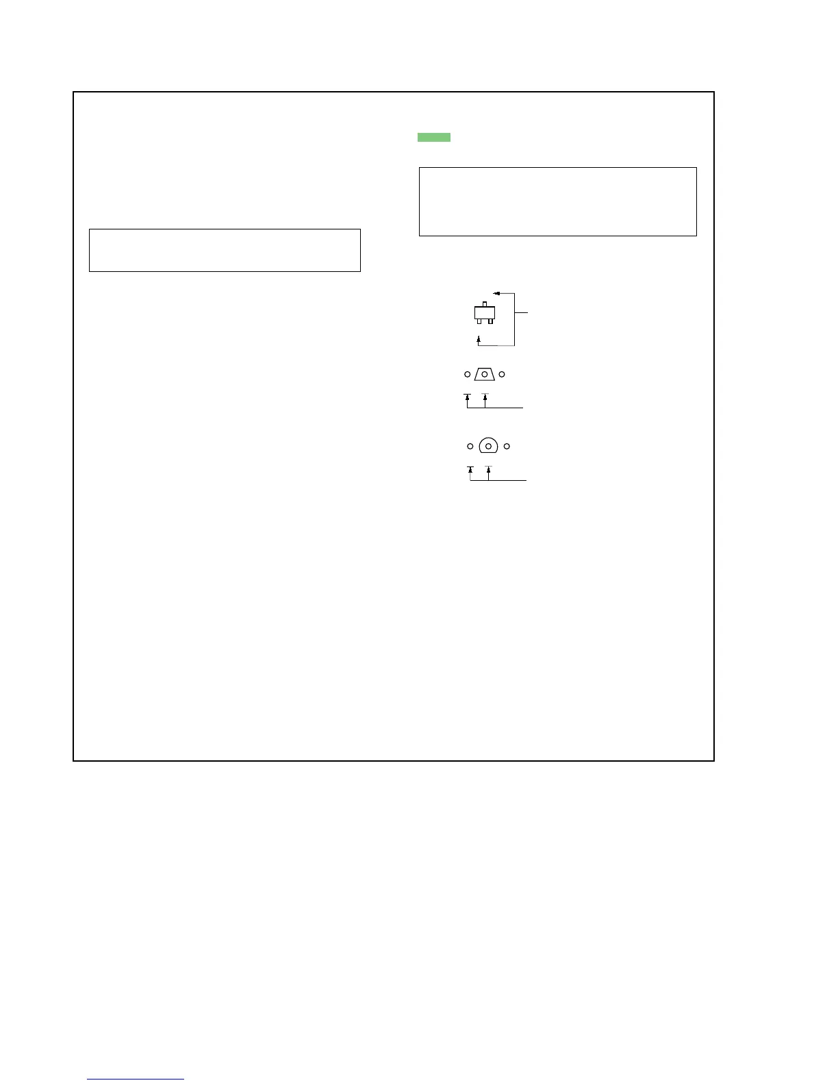
• Indication of transistor.
• Abbreviation
E2 : 120V AC Area in E model
E3 : 240V AC Area in E model
EA : Saudi Arabia mdoel
E15 : Iran model
SP : Shingapore model
MY : Malaysia model
TH : Thai model
Caution:
Parts face side: Parts on the parts face side seen from
(Side A) the parts face are indicated.
Pattern face side: Parts on the pattern face side seen from
(Side B) the pattern face are indicated.
C
B
These are omitted.
E
Q
B
These are omitted.
CE
Q
B
These are omitted.
CE
Q
Note on Printed Wiring Boards:
• X : parts extracted from the component side.
• : Pattern from the side which enables seeing.