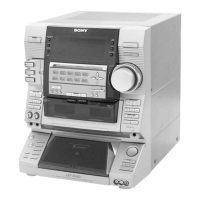
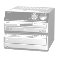
HCD-SHAKE7
63
Pin No. Pin Name I/O Description
52 O-ANALOG-BSEL O Multiplexer selector B for Analog input
53 NO-USE - Not used
54 NO-USE - Not used
55 O-MTK-RESET O MTK Reset pin
56 I-MTK-XIFCS I MTK CHIP SELECT
57 O-MTK-BUSY O BUSY Signal communication between MTK
58 O-CD-MOTOR + O CDM turning motor control signal output
59 O-CD-MOTOR - O CDM turning motor control signal output
60 VCC2 I Power supply terminal (+3.3V)
61 MFISW - Not used
62 VSS I Ground terminal
63 I-CDM-SW-A I CDM LOAD SW
64 I-CDM-SW-B I CDM UNLOAD SW
65 I-AD-KEY0 I Key input terminal (A/D input)
66 I-DSP-INT I DSP Initialization completion interupt signal
67 O-DSP-MUTE O DSP Mute control . "H": Mute On
68 /I-FAN-BLOCK-DET I Fan Block Detection Pin. "L": Block On
69 I-FAN-SPEED I Fan speed control input signal. "L": High speed
70 /I-THERMISTOR-DET I Temperature protect pin. "L": Protect on
71 /I-DC-DET I DC detection pin. "L": Protect on
72 I-DAMP-OCP I Digital Amp over current protection pin. "L": Protect on
73 O-DAMP-RESET O Digital Amp Reset Pin
74 /I-SD-FAST I Power Supply Shutdown Protection Detection Pin. "L": Protect on
75 I-DSP-SDA I DSP IC: Data signal for IIC communcation
76 I-DSP-SCL I DSP IC: Clock signal for IIC communcation
77 O-PCONT-7V-13.5V O 13.5V & 7V Power Switch Control pin. "H": 13V
78 O-PCONT-DAMP O Digital Amp Module Power Control Pin. "H": ON
79 O-MTK-POWER-CTRL O Power Control pin for MTK
80
O-RGB-TRANS-LED-
SPK
O Transfer signal to RGB driver (driver for Speaker LED)
81
I-MTK-POWER-MONITOR
- Not used
82 NO-USE - Not used
83 NO-USE - Not used
84 O-VBUS-OE O MTK Vbus Output enable control pin
85 /I-HUB-OC-USB-B I USB Overcurrent Detection input port B
86 /I-HUB-OC-USB-A I USB Overcurrent Detection input port A
87 O-HUB-VBUS-DETECT O Hub Power (V-DET) Control Port
88 O-HUB-RESET O MTK Hub reset pin
89 I-AD-KEY2 I Key input terminal (A/D input)
90 I-AD-KEY1 I Key input terminal (A/D input)
91 I-MIC-DETECT I Mic Input Detection pin. "H": Mic detected
92 I-MASTER-VOLUME I Jog dial pulse input from the MASTER VOLUME encoder (A/D input)
93 O-PCONT-BTSTBY O BT Standby Power Control Pin. "H": ON
94 AVSS I Ground terminal
95 I-MODEL-DEST-IN I Model and Destination setting terminal (A/D input)
96 VREF I A/D Converter reference voltage input terminal (+3.3V)
97 AVCC I Power supply terminal (+3.3V)
98 O-FL-LATCH O Data Latch signal to FL CIG
99 O-FL-SOUT O Serial data output to FL CIG
100 O-FL-CLK O Serial clock output to FL CIG