81
HCD-SR4W
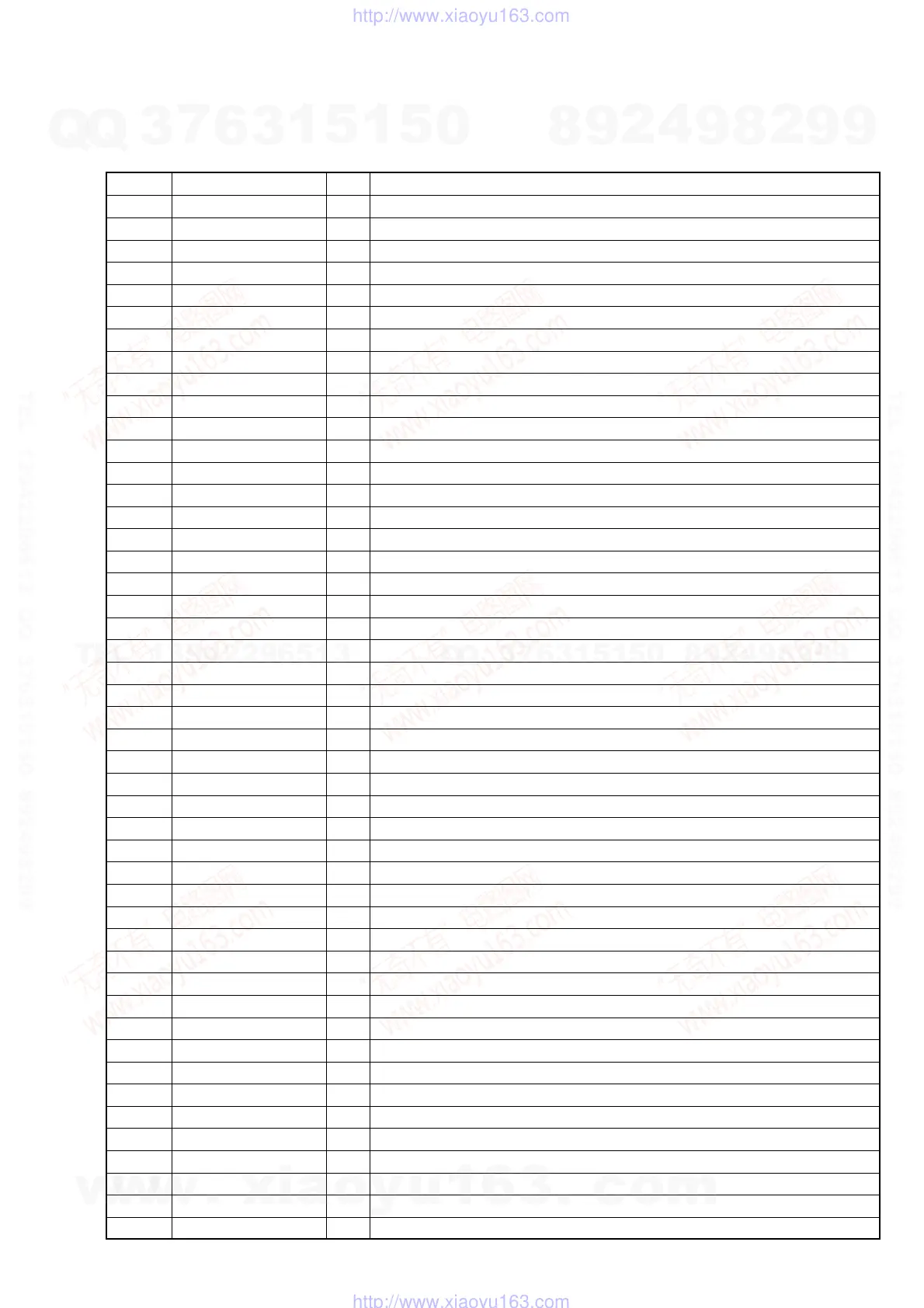
• IC Pin Function Description
DMB08 BOARD IC206 ZIVA5X-C2F (DVD SYSTEM PROCESSOR)
Pin No. Pin Name I/O Description
1 VDDP — Power supply terminal (+3.3V) (I/O signal)
2 HA1 I/O Address bus
3 HD15 I/O Data bus (address signal multiplexed)
4 HD14 I/O Data bus (address signal multiplexed)
5 HD13 I/O Data bus (address signal multiplexed)
6 HD12 I/O Data bus (address signal multiplexed)
7 HD11 I/O Data bus (address signal multiplexed)
8 HD10 I/O Data bus (address signal multiplexed)
9 HD9 I/O Data bus (address signal multiplexed)
10 HD8 I/O Data bus (address signal multiplexed)
11 HD7 I/O Data bus (address signal multiplexed)
12 VDDP — Power supply terminal (+3.3V) (I/O signal)
13 GNDP — Ground terminal (I/O signal)
14 HD6 I/O Data bus (address signal multiplexed)
15 HD5 I/O Data bus (address signal multiplexed)
16 HD4 I/O Data bus (address signal multiplexed)
17 HD3 I/O Data bus (address signal multiplexed)
18 HD2 I/O Data bus (address signal multiplexed)
19 HD1 I/O Data bus (address signal multiplexed)
20 VDDP — Power supply terminal (+3.3V) (I/O signal)
21 GNDP — Ground terminal (I/O signal)
22 HD0 I/O Data bus (address signal multiplexed)
23 HDTACK I/O Acknowledge signal input/output for host data transfer (not used)
24 HIRQ0 I Interrupt signal input for Medusa (not used)
25 WEH.UDS I/O Host upper data strobe signal output
26 WEL.LDS I/O Host lower data strobe signal output (not used)
27 HREAD I/O Read/write strobe signal output
28 GPIO0 I/O Jig detection port (pull-up)
29 GND — Ground terminal (inside core)
30 VDD — Power supply terminal (+1.8V) (inside core)
31 GND25 — Ground terminal (SDRAM I/O signal)
32 VDD25 — Power supply terminal (+3.3V) (SDRAM I/O signal)
33 MA9 O SDRAM address bus
34 MA8 O SDRAM address bus
35 MA7 O SDRAM address bus
36 MA6 O SDRAM address bus
37 MA5 O SDRAM address bus
38 MA4 O SDRAM address bus
39 MA3 O SDRAM address bus
40 MA2 O SDRAM address bus
41 MA1 O SDRAM address bus
42 MA0 O SDRAM address bus
43 GND25 — Ground terminal (SDRAM I/O signal)
44 VDD25 — Power supply terminal (+3.3V) (SDRAM I/O signal)
45 MA10 O SDRAM address bus
46 MA11 O SDRAM address bus
47 BA1 O SDRAM bank select 1 signal output
w
w
w
.
x
i
a
o
y
u
1
6
3
.
c
o
m
Q
Q
3
7
6
3
1
5
1
5
0
9
9
2
8
9
4
2
9
8
T
E
L
1
3
9
4
2
2
9
6
5
1
3
9
9
2
8
9
4
2
9
8
0
5
1
5
1
3
6
7
3
Q
Q
TEL 13942296513 QQ 376315150 892498299
TEL 13942296513 QQ 376315150 892498299
http://www.xiaoyu163.com
http://www.xiaoyu163.com