76
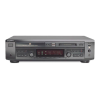
MXD-D40
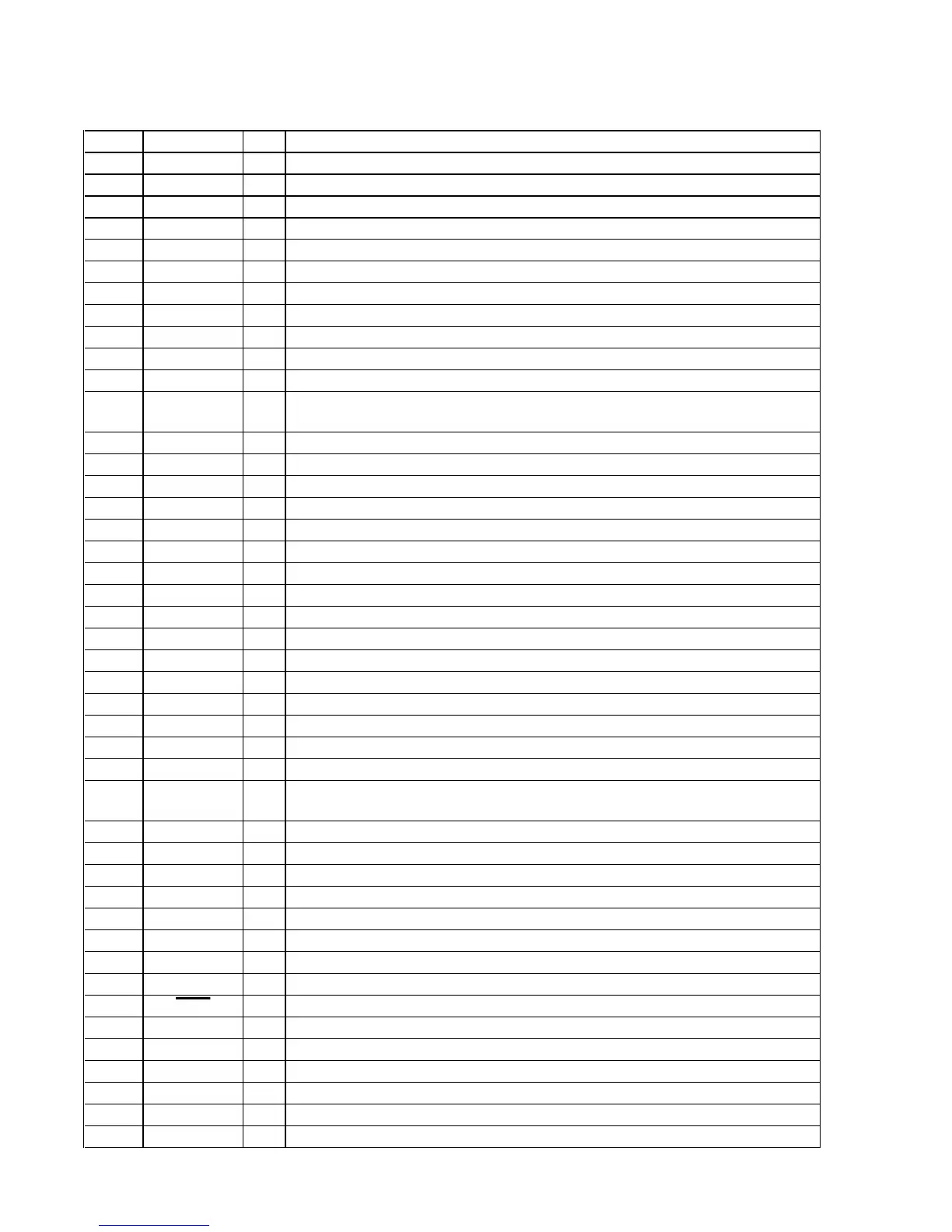
• MAIN BOARD IC800 M30624MGA-A54FP (SYSTEM CONTROLLER (CD MECHANISM CONTROLLER))
Pin No. Pin Name I/O Description
1 CD-DATA
O Serial data output to the CD block
2 CD-CLK
O Serial data transfer clock signal output to the CD block
3 XLT
O Serial data latch pulse signal output to the CD block
4 SIRCS
I Remote control signal input from the remote control receiver (IC781)
5NC
O Not used (open)
6
SQ-DATA
I
Subcode Q data input from the CD block
7
S-QCLK
O
Subcode Q data reading clock signal output to the CD block “L”: active
8BYTE
I External data bus line byte selection signal input “L”: 16 bit, “H”: 8 bit (fixed at “L”)
9 CNVSS
— Ground terminal
10 HOLD
O Laser power control signal output terminal Not used (open)
11 SENS
I Internal status (SENSE) input from the CD block
12 RESET I
System reset signal input from the reset signal generator (IC505) “L”: reset
For several hundreds msec. after the power supply rises, “L” is input, then it changes to “H”
13 X-OUT
O Main system clock output terminal (10 MHz)
14 VSS
— Ground terminal
15 X-IN
I Main system clock input terminal (10 MHz)
16 VCC
— Power supply terminal (+5V)
17
NMI I Non-maskable interrupt input terminal “L” active (fixed at “H” in this set)
18 P_DOWN
I Power down detection signal input terminal “L”: power down, normally: “H”
19 SCOR
I Subcode sync (S0+S1) detection signal input from the CD block “H”: active
20 TP
O Not used (open)
21 EXT_ON
I EXT_ON input terminal
22 CONNECT
I Connect signal input terminal
23 TP
O Not used (open)
24 LINE_MUTE O
Audio line muting on/off control signal output “L”: line muting on
25 LDON O
Laser diode on/off control signal output to the automatic power control circuit “H”: laser on
26 MD_RST
O Reset signal output to the system controller (IC801)
27 DAC_MUTE
O Muting control signal output to the D/A converter (IC300)
28 TP
O Not used (open)
29 IIC-CLK
I/O
Communication data reading clock signal output or transfer clock signal input with the system
controller (IC801)
30 IIC-DATA I/O
Communication data bus with the system controller (IC801)
31 TXD1 O
Not used (open)
32 RXD1 O
Not used (open)
33 CLK1 O
Not used (open)
34 RTS1 O
Not used (open)
35
FLWITE O Serial data output to the display controller (IC751)
36 FLREAD
I Not used (fixed at “L”)
37 FLCLK
O Serial data transfer clock signal output to the display controller (IC751)
38 FLCS
O Serial data transfer request signal output to the display controller (IC751)
39 FLREQ
O Serial data transfer request signal input terminal Not used (open)
40 FLBUSY
O Serial data transfer permission signal input terminal Not used (open)
41 NC
O Not used (fixed at “L”)
42 1-4
O Disc speed selection (normal/4 speed) signal output to the CD block
43 1-2
O Disc speed selection (normal/2 speed) signal output to the CD block
44
8-12 O Disc size selection signal output to the CD block Not used (open)
 Loading...