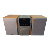
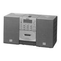
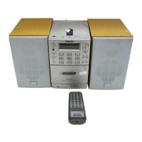
PMC-DR45L
– 35 – – 36 –
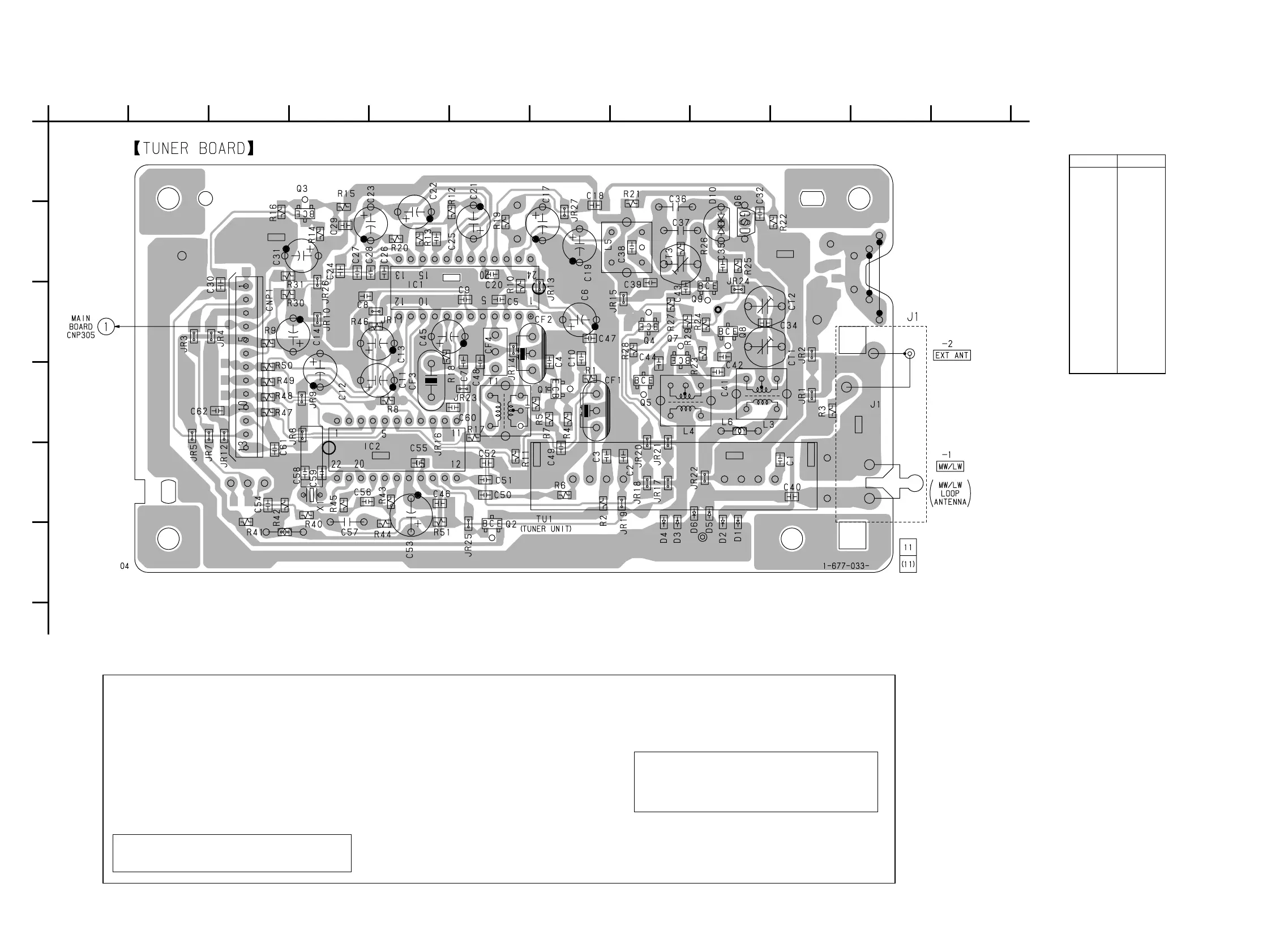
6-7. PRINTED WIRING BOARD — TUNER SECTION —
1
A
B
C
D
E
F
23456789101112
TP
(VT)
D1 F-9
D2 F-9
D3 F-8
D4 F-8
D5 F-9
D6 F-9
D10 B-9
IC1 C-5
IC2 E-5
Q1 D-7
Q2 E-6
Q3 A-4
Q4 C-8
Q5 D-8
Q6 B-9
Q7 C-8
Q8 C-9
Q9 C-9
• Semiconductor
Location
Ref. No. Location
(Page 47)
THIS NOTE IS COMMON FOR PRINTED WIRING
BOARDS AND SCHEMATIC DIAGRAMS.
(In addition to this, the necessary note is
printed in each block.)
for Schematic Diagram:
• All capacitors are in µF unless otherwise noted. pF: µµF
50 WV or less are not indicated except for electrolytics
and tantalums.
• All resistors are in Ω and
1
/
4
W or less unless otherwise
specified.
• % : indicates tolerance.
•
f
: internal component.
• C : panel designation.
Note: The components identified by mark 0 or dotted line
with mark 0 are critical for safety.
Replace only with part number specified.
Caution:
Pattern face side: Parts on the pattern face side seen from
(Conductor Side) the pattern face are indicated.
Parts face side: Parts on the parts face side seen from
(Component Side) the parts face are indicated.
• U : B+ Line.
• V : B– Line.
• H : adjustment for repair.
• Voltages are taken with a VOM (Input impedance 10 MΩ).
Voltage variations may be noted due to normal produc-
tion tolerances.
• Waveforms are taken with a oscilloscope.
Voltage variations may be noted due to normal produc-
tion tolerances.
• Circled numbers refer to waveforms.
• Signal path.
F : FM
f : MW/LW
L : LINE
E : PB
a : REC
J : CD
c : digital out
for Printed Wiring Boards:
• X : parts extracted from the component side.
• Y : parts extracted from the conductor side.
•
a
: Through hole.
• b : Pattern from the side which enables seeing.
(The other layer’s patterns are not indicated.)