2
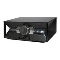
SS-SHAKE99/SHAKE100
SECTION 1
DIAGRAMS
For Schematic Diagrams.
Note:
•
C
: panel designation.
• Signal path
F
:
AUDIO
THIS NOTE IS COMMON FOR PRINTED WIRING BOARDS AND SCHEMATIC DIAGRAMS.
(In addition to this, the necessary note is printed in each block.)
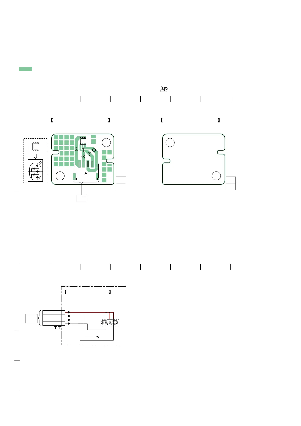
For Printed Wiring Boards.
Note:
•
X
: Parts extracted from the component side.
•
: Pattern from the side which enables seeing.
(The other layers' patterns are not indicated.)
1-1. PRINTED WIRING BOARD –
SPK RGB LED
Board
–
•
: Uses unleaded solder.
1-2. SCHEMATIC DIAGRAM – SPK RGB LED Board –
1
A
B
C
D
2 3 4 5 6 78
D3600
14
CN3600
CL3600
CL3601
CL3602
CL3603
R3601
SPK RGB LED BOARD
(COMPONENT SIDE)
1-889-619-
11
(11)
SPK RGB LED BOARD
(CONDUCTOR SIDE)
1-889-619-
11
(11)
GA
RA
BA
GK
RK
BK
GK
BK
RK
GA
BA
RA
D3600
LED
SPEAKER
L/R
1
A
B
C
D
2 3 4 5 6 78
SPK RGB LED BOARD
CL3602
CL3600
CL3601
CL3603
4P
CN3600
M+5.2V 1
2RED_LED
3BLUE_LED
GREEN_LED 4
BLU
RED
GRN
SMLVN6RGB1U17QYB
D3600
22
R3601
LED
SPEAKER
L/R
Ver. 1.1