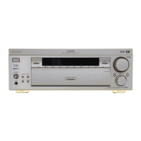
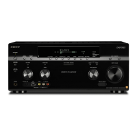
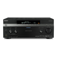
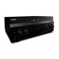
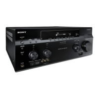
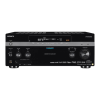
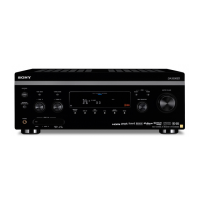
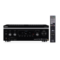
STR-DA5400ES
128
Pin No. Pin Name I/O Description
55 ERR - Not used
56 GND - Ground terminal
57 MIDDLE O Buffer status output to the system controller
58 EMPTY O Not used
59 FULL O Not used
60 - - Not used
61 GND - Ground terminal
62 VCCINT - Power supply terminal (+1.2V)
63 - - Not used
64 MODE I Not used
65 MUTE I Muting control signal input from the system controller
66 VCCIO4 - Power supply terminal (+3.3V)
67 OUTPUTEN I Not used
68 GND - Ground terminal
69 MEMCLR I Not used
70 TXSTART I Not used
71 RXSTART I Not used
72 SDA I/O
I2C data bus with the D/A converter (for audio section), system controller and video input
selector
73 BA1 O Bank address signal output terminal Not used
74 BA0 O Bank address signal output to the SD-RAM
75 INIT_DONE - Not used
76 XCS O Chip select signal output to the SD-RAM
77 VCCIO3 - Power supply terminal (+3.3V)
78 GND - Ground terminal
79 XRAS O Row address signal output to the SD-RAM
80 XCAS O Column address signal output to the SD-RAM
81 XWE O Write enable signal output to the SD-RAM
82
∗nSTATUS
- Confi guration status terminal Not used
83
∗CONF_DONE
O Confi guration status output terminal
84, 85
∗MSEL1, ∗MSEL0
I Mode setting terminal
86 LDQM O Data mask signal output to the SD-RAM (lower byte)
87 - - Not used
88 SCL I I2C clock signal input from the system controller
89 - - Not used
90 SYSCLK I System clock signal input terminal
91 - - Not used
92 to 94 A0 to A2 O Address signal output to the SD-RAM
95 VCCIO3 - Power supply terminal (+3.3V)
96, 97 A3, A4 O Address signal output to the SD-RAM
98 GND - Ground terminal
99 to 101 A5 to A7 O Address signal output to the SD-RAM
102 VCCIO3 - Power supply terminal (+3.3V)
103, 104 A8, A9 O Address signal output to the SD-RAM
105 GND - Ground terminal
106 GND_PLL2 - Ground terminal (for PLL)
107 VCCD_PLL2 - Power supply terminal (+1.2V) (digital system) (for PLL)
108 GND_PLL2 - Ground terminal (for PLL)
109 VCCA_PLL2 - Power supply terminal (+1.2V) (analog system) (for PLL)
110 GNDA_PLL2 - Ground terminal (analog system) (for PLL)
111 GND - Ground terminal
112 A10 O Address signal output to the SD-RAM
113 A11 O Address signal output terminal Not used
114, 115 D0, D1 I/O Two-way data bus with the SD-RAM
116 VCCIO2 - Power supply terminal (+3.3V)
117 GND - Ground terminal
w
w
w
.
x
i
a
o
y
u
1
6
3
.
c
o
m
Q
Q
3
7
6
3
1
5
1
5
0
9
9
2
8
9
4
2
9
8
T
E
L
1
3
9
4
2
2
9
6
5
1
3
9
9
2
8
9
4
2
9
8
0
5
1
5
1
3
6
7
3
Q
Q
TEL 13942296513 QQ 376315150 892498299
TEL 13942296513 QQ 376315150 892498299
http://www.xiaoyu163.com
http://www.xiaoyu163.com
