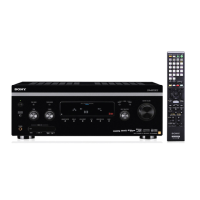
STR-DA5400ES
149
Pin No. Pin Name I/O Description
A1 NC - Not used
A2 MSTR1_SDA O Power detection signal output to the video system controller
A3 MSTR1_SCL O Busy signal output to the video system controller
A4, A5 FSDATA1, FSDATA3 I/O Two-way data bus with the SD-RAM
A6 FSDQM0 O Data mask signal output to the SD-RAM (upper byte)
A7 to A10
FSDATA5, FSDATA7,
FSDATA9, FSDATA11
I/O Two-way data bus with the SD-RAM
A11 FSDQM1 O Data mask signal output to the SD-RAM (lower byte)
A12, A13
FSDATA13,
FSDATA15
I/O Two-way data bus with the SD-RAM
A14 VDDA18_DLL - Power supply terminal (+1.8V)
A15, A16
FSDATA17,
FSDATA19
I/O Two-way data bus with the SD-RAM
A17 FSDQS2 O Data strobe signal output to the SD-RAM (upper byte)
A18 to A21
FSDATA21, FSDATA23,
FSDATA25, FSDATA27
I/O Two-way data bus with the SD-RAM
A22 FSDQS3 O Data strobe signal output to the SD-RAM (lower byte)
A23, A24 FSDATA29, FSDATA31 I/O Two-way data bus with the SD-RAM
A25, A26 RPLL_AGND - Ground terminal
B1 BDATA0 I Digital video signal input terminal Not used
B2 OCM_UDO_1 O Serial data output to the video system controller
B3 OCM_UDI_1 I Serial data input from the video system controller
B4, B5 FSDATA0, FSDATA2 I/O Two-way data bus with the SD-RAM
B6 FSDQS0 O Data strobe signal output to the SD-RAM (upper byte)
B7 to B10
FSDATA4, FSDATA6,
FSDATA8, FSDATA10
I/O Two-way data bus with the SD-RAM
B11 FSDQS1 O Data strobe signal output to the SD-RAM (lower byte)
B12, B13 FSDATA12, FSDATA14 I/O Two-way data bus with the SD-RAM
B14 VSSA18_DLL - Ground terminal
B15, B16 FSDATA16, FSDATA18 I/O Two-way data bus with the SD-RAM
B17 FSDQM2 O Data mask signal output to the SD-RAM (upper byte)
B18 to B21
FSDATA20, FSDATA22,
FSDATA24, FSDATA26
I/O Two-way data bus with the SD-RAM
B22 FSDQM3 O Data mask signal output to the SD-RAM (lower byte)
B23, B24 FSDATA28, FSDATA30 I/O Two-way data bus with the SD-RAM
B25 RPLL_DGND - Ground terminal
B26 XTAL O System clock output terminal Not used
C1 to C3 BDATA3 to BDATA1 I Digital video signal input terminal Not used
C4 FSCKE O Clock enable signal output to the SD-RAM
C5 FSCLKN O Clock signal (negative) output to the SD-RAM
C6 to C8 FSADDR8 to FSADDR6 O Address signal output to the SD-RAM
C9 FSVREF O Reference voltage output to the SD-RAM
C10 to
C18
FSADDR5, FSADDR12,
FSADDR9, FSADDR4,
FSADDR11, FSADDR3
to FSADDR0
O Address signal output to the SD-RAM
C19 FSVREF O Reference voltage output to the SD-RAM
C20, C21 FSBKSEL1, FSBKSEL0 O Bank select signal output to the SD-RAM
C22 FSCS1 O Chip select signal output terminal Not used
C23 FSWE O Write enable signal output to the SD-RAM
C24 FSRAS O Row address strobe signal output to the SD-RAM
C25 RPLL_1.8V - Power supply terminal (+1.8V)
C26 TCLK I System clock input terminal (19.6608 MHz)
D1 to D3 BDATA6to BDATA4 I Digital video signal input terminal Not used
D4 DDR_2.5V - Power supply terminal (+2.5V)
D5 FSCLKP O Clock signal (positive) output to the SD-RAM
D6 to D8 DDR_2.5V - Power supply terminal (+2.5V)
D VIDEO BOARD IC3606 FLI8638-LF (VIDEO PROCESSOR2)
w
w
w
.
x
i
a
o
y
u
1
6
3
.
c
o
m
Q
Q
3
7
6
3
1
5
1
5
0
9
9
2
8
9
4
2
9
8
T
E
L
1
3
9
4
2
2
9
6
5
1
3
9
9
2
8
9
4
2
9
8
0
5
1
5
1
3
6
7
3
Q
Q
TEL 13942296513 QQ 376315150 892498299
TEL 13942296513 QQ 376315150 892498299
http://www.xiaoyu163.com
http://www.xiaoyu163.com